Light emitting device

a technology of light emitting device and glass film, which is applied in the direction of solid-state devices, semiconductor devices, lighting and heating apparatus, etc., can solve the problems of low gas barrier performance, poor gas barrier performance of glass film, and poor heat resistance of plastic materials with excellent weathering resistance, etc., and achieve no deterioration in light reflecting performance and high gas barrier performance

Active Publication Date: 2009-01-08
NICHIA CORP
View PDF14 Cites 39 Cited by
  • Summary
  • Abstract
  • Description
  • Claims
  • Application Information

AI Technical Summary

Benefits of technology

[0010]The light emitting device of the present invention has a glass film with Si—N bonds as an essential component, which provide high gas barrier performance, between the translucent resin and the metal reflecting member provided at a location that will be directly affe...

Problems solved by technology

However, the glass sealed body formed by hydrolytic polymerization by sol-gel method is formed much thicker than the thickness of a light emitting element, and it is therefore believed to be susceptible to cracking due to shrinkage in the course of molding, and such glass film has extremely poor gas barrier performance.
However, plastic materials with excellent resistance to heat and weathering tend to h...

Method used


Image

  • Light emitting device
  • Light emitting device

Examples


Embodiment Construction

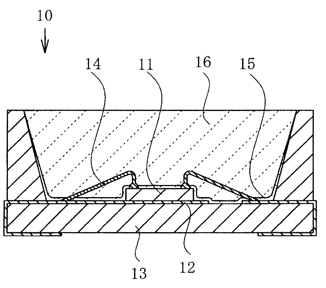
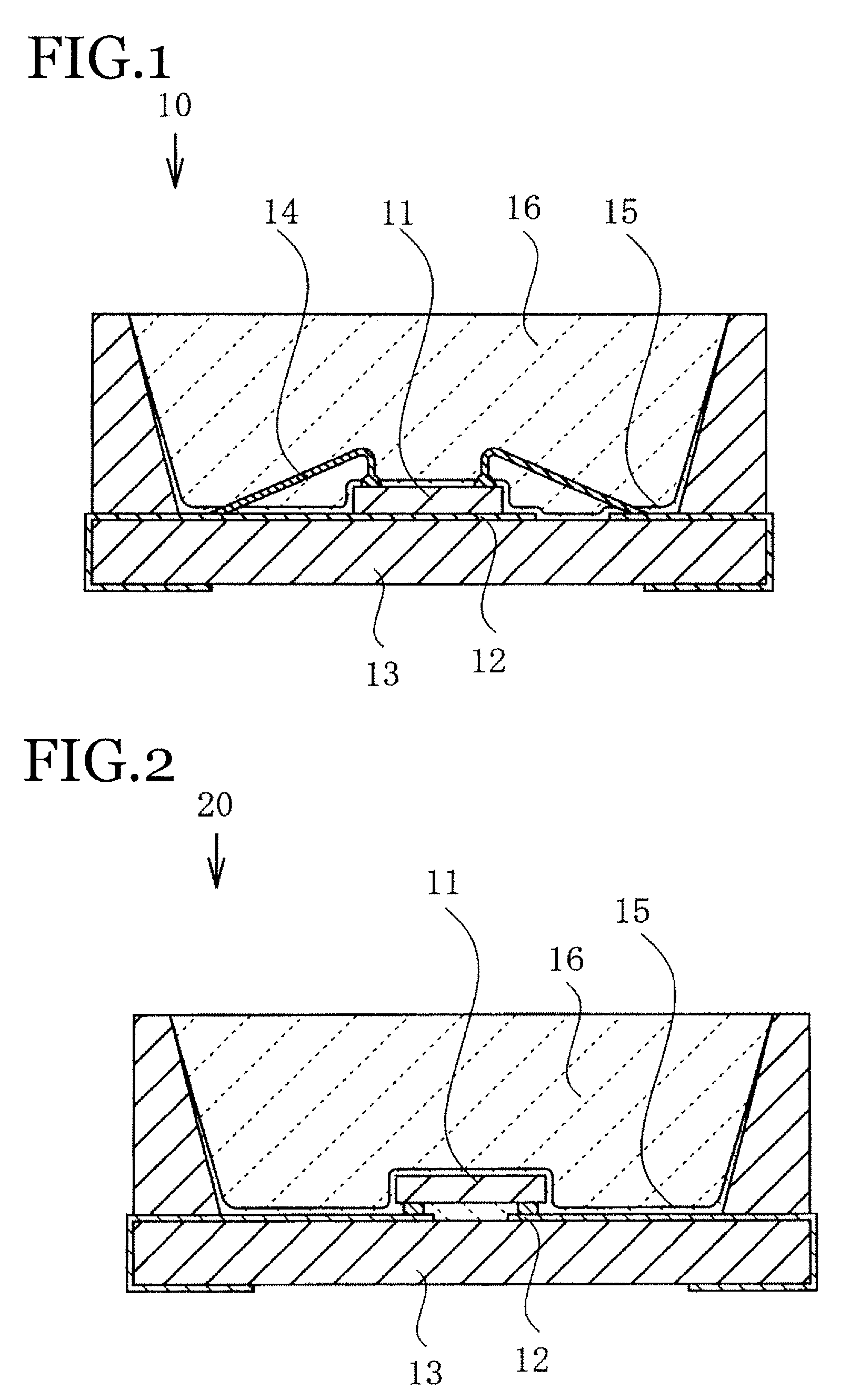
[0013]The best mode for carrying out the invention will now be described through reference to the drawings, but the mode described below merely exemplifies a semiconductor device manufacturing method for embodying the technological concepts of the present invention, and the present invention is not limited to the semiconductor device manufacturing method discussed below.

[0014]Also, this Specification does not limit the members given in the Claims to the members of the embodiments. The sizes, materials, shapes, relative disposition, and so forth of the constituent members discussed in the embodiments are not unless, otherwise specified, intended to limit the scope of the invention to just those, and are merely given as descriptive examples. Furthermore, the size, positional relationships, and so forth of the members illustrated in the various diagrams may be exaggerated in order to make the description more clear.

[0015]Further, in the following description, members that are the same ...


PUM


Abstract

A light emitting device comprises; a metal reflecting member, a light emitting element fixed to the metal reflecting member, a glass film that covers the metal reflecting member and has Si—N bonds, and a translucent resin that covers the glass film. The present invention provides a light emitting device with which, even when this device is used in a harsh environment, there will be no deterioration in the light reflecting performance of the metal reflecting member, and light can be emitted at high output over an extended period.

Description

BACKGROUND OF THE INVENTION[0001]1. Field of the Invention[0002]This invention relates to a light emitting device sealed a light emitting element with translucent sealing material.[0003]2. Background Information[0004]There has been a variety of proposals for light emitting devices in which lighting source is a light emitting element. For instance, a light emitting device in which a glass material covers a light emitting element and close thereto (see JP-2000-299503-A).[0005]However, the glass sealed body formed by hydrolytic polymerization by sol-gel method is formed much thicker than the thickness of a light emitting element, and it is therefore believed to be susceptible to cracking due to shrinkage in the course of molding, and such glass film has extremely poor gas barrier performance.[0006]When a light emitting device is to be used in a harsh environment, it is common for the plastic material that is used to be one with excellent resistance to heat and weathering. However, plas...

Claims


Application Information

Patent Timeline
IPC IPC(8): F21V7/22
CPCH01L33/44H01L33/60H01L2224/16225H01L2224/48091H01L2224/48465H01L2224/8592H01L2924/3025H01L2924/00014H01L2924/00H01L2924/181H01L2924/00012
Inventor HAYASHI, TADAOTAMAKI, HIROTOHOSOKAWA, SHOJISHIMIZU, YASUNORI
Owner NICHIA CORP
Why Eureka
Try Eureka