Gas barrier thin film laminate, gas barrier resin substrate and organic el device
- Summary
- Abstract
- Description
- Claims
- Application Information
AI Technical Summary
Benefits of technology
Problems solved by technology
Method used
Image
Examples
example 1
Manufacture of Electrode
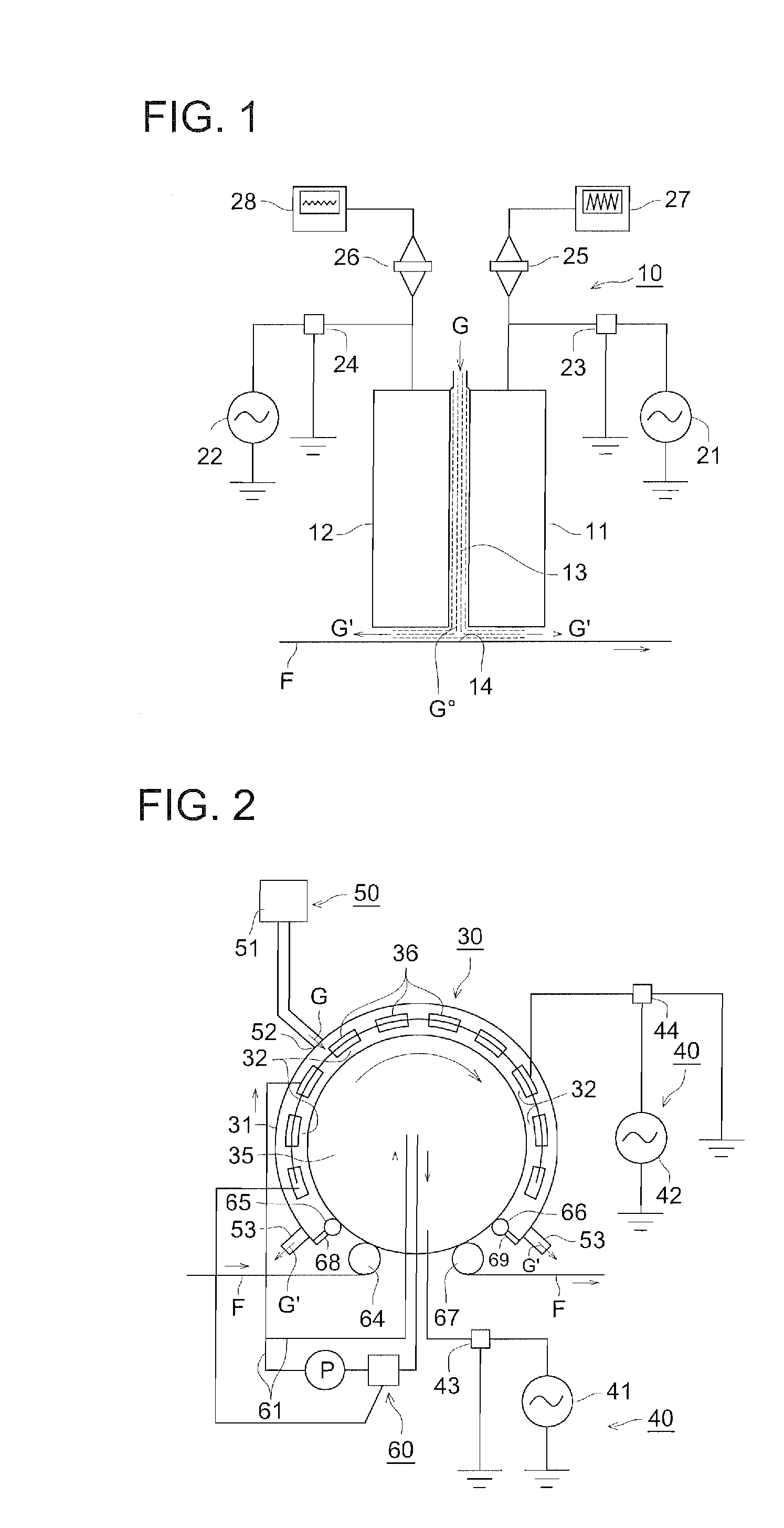
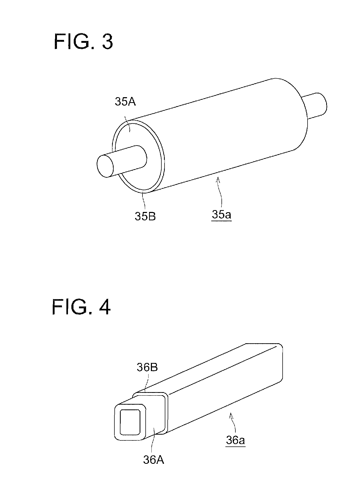
[0239]Using the atmospheric pressure plasma discharge processing apparatus of FIG. 2, a roll electrode covered with a dielectric and a plurality of rectangular electrodes also covered with a dielectric were manufactured as a set according to the following procedure:
[0240]The roll electrode to be made into a first electrode was manufactured in such a way that a jacket roll metallic base material of titanium alloy T64 having a means to keep a predetermined temperature was covered with an alumina thermal spray-coated film of higher density and closer adhesion according to the atmospheric plasma method to have a roll diameter of 1000 mm.
[0241]The dielectric surface provided with pore sealing coating was ground to a surface roughness of Rmax 5 μm. The final dielectric void ratio (void ratio of sufficient penetrability) was almost 0% by volume, the percentage of SiOx content in the dielectric layer at this time was 75 mol %, the final dielectric film thickness was ...
example 2
Manufacture of Sample 7
[0341]Sample 7 was manufactured in the same procedure as that of the aforementioned sample 1, except that the layer was designed in the structure of resin substrate / stress relaxation film / inorganic film / stress relaxation film / inorganic film / stress relaxation film and the stress relaxation film forming conditions were modified as follows: The stress relaxation film was 200 nm thick, and inorganic film was 50 nm thick.
[0342]
[0343]Electrical discharge gas: nitrogen gas: 94.4% by volume
[0344]Thin film forming gas: hexamethyl disiloxane: 0.1% by volume
[0345]Thin film forming gas: neopentyl glycolate diacrylate: 0.5% by volume
[0346]Additive gas: methane gas: 5.0% by volume
[0347]
[0348]Power source on the first electrode side: A5
[0349]Frequency: 100 kHz
[0350]output power density: 10 W / cm2 (Voltage Vp was 7 kV in this case)
[0351]Electrode temperature: 120° C.
[0352]Power source on the second electrode side: B3
[0353]Frequency: 13.56 MHz
[0354]output power density: 5 W / cm2...
example 3
Manufacture of Sample 9
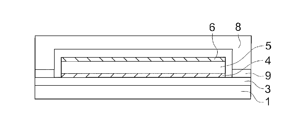
[0366]Thin films were formed sequentially on the OLED laminated with 0.5 mm thick alkali-free glass (1737 by Corning), a transparent electrode constituting the anode electrode, a positive hole transport layer for transporting a positive hole, a light emitting layer, an electron injection layer, and a rear surface electrode as a cathode, under the following manufacturing conditions using an atmospheric pressure plasma discharge processing apparatus of FIG. 1. A gas barrier thin film laminate (stress relaxation film; 200 nm thick, inorganic film; 50 nm thick) having a structure of OLED / stress relaxation film / inorganic film / stress relaxation film / inorganic film / stress relaxation film was formed, whereby the sample 9 was produced.
[0367]Stress relaxation film gas mixture composition
[0368]Electrical discharge gas: nitrogen gas: 94.4% by volume
[0369]Thin film forming gas: tetraethoxy silane: 0.1% by volume
[0370]Thin film forming gas: methyl methacrylate: 0.5% by volu...
PUM
| Property | Measurement | Unit |
|---|---|---|
| Fraction | aaaaa | aaaaa |
| Glass transition temperature | aaaaa | aaaaa |
| Volume | aaaaa | aaaaa |
Abstract
Description
Claims
Application Information


