Toggle Magnetic Random Access Memory and Write Method of Toggle Magnetic Random Access Memory
a write method and magnetic random access technology, applied in the field write method of can solve the problems of data stored in memory cell b that cannot be rightly sensed, the possibility of erroneous writing is very low, and the execution of the continuous burst write operation of the toggle magnetic random access memory is very difficult, so as to achieve the effect of not affecting the reliability and increasing the circuit area
- Summary
- Abstract
- Description
- Claims
- Application Information
AI Technical Summary
Benefits of technology
Problems solved by technology
Method used
Image
Examples
first embodiment
[0090]At first, the configuration in the first embodiment of the toggle MRAM of the present invention will be explained.
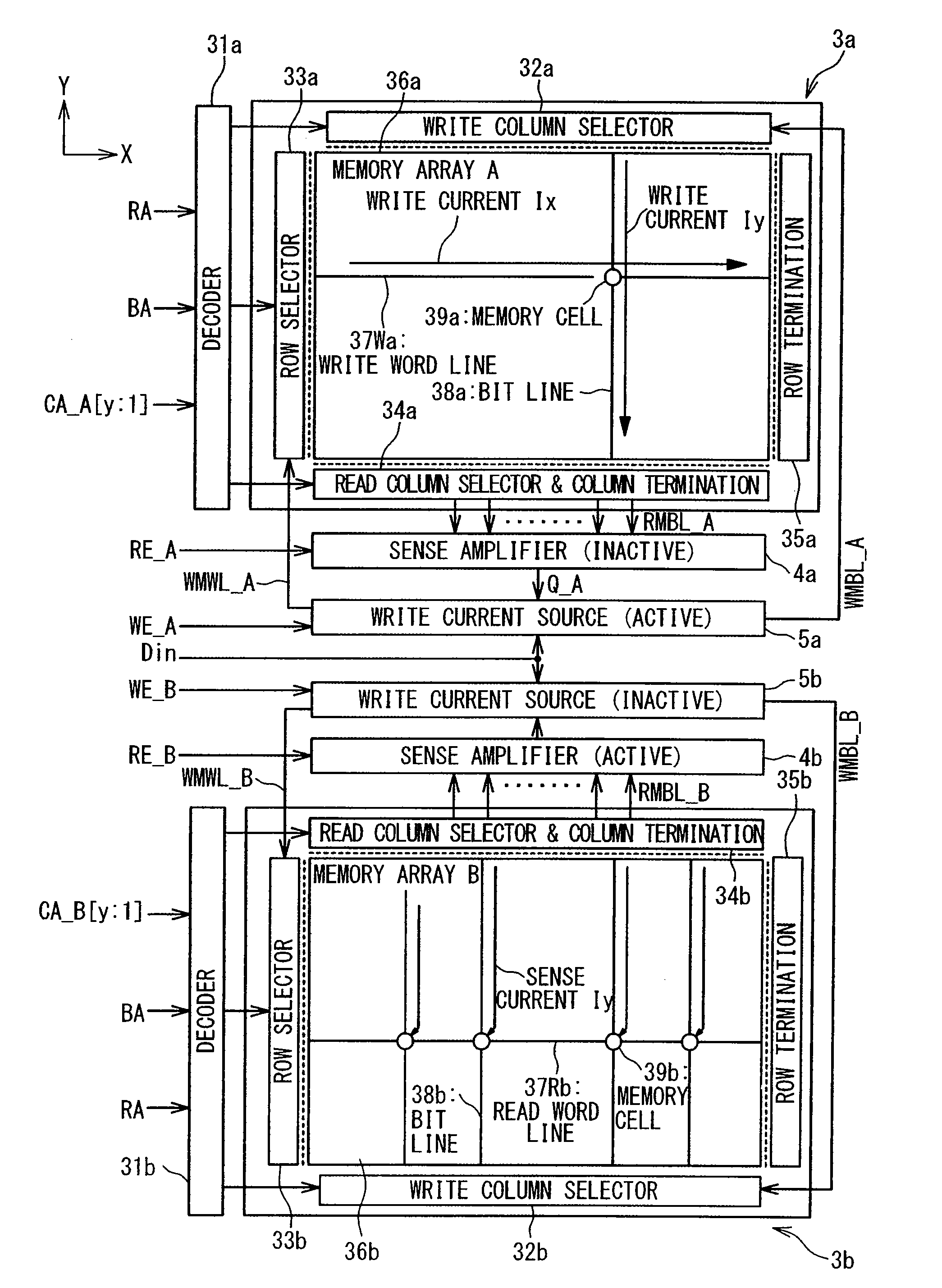
[0091]FIG. 9 is a block diagram showing a configuration in the first embodiment of the toggle MRAM of the present invention. A toggle MRAM 1 includes a controller 2, a decoder & memory array A 3a, a decoder & memory array B 3b, a sense amplifier A 4a, a sense amplifier B 4b, a write circuit A 5a, a write circuit B 5b, a multiplexer 6.
[0092]The decoder & memory array A 3a includes a memory array A 36a having a plurality of memory cells 39a that are arranged in a matrix shape. The decoder & memory array B 3b includes the memory array A 36a having a plurality of memory cells 39b that are arranged in a matrix shape. Write word lines 37W and bit lines 38 of the memory array A 36a are physically separated from those of the memory array B 36b. Its detail will be described later.
[0093]The controller 2 controls the decoder & memory array A 3a and the decoder & memory array ...
second embodiment
[0137]The configuration in the second embodiment of the toggle MRAM of the present invention will be described below.
[0138]FIG. 15 is a block diagram showing a configuration in the second embodiment of the toggle MRAM of the present invention. A toggle MRAM 61 includes a controller 62, a decoder & memory array A 63a, a decoder & memory array B 63b, a sense amplifier 64, a write circuit 65, a selector 66 and OR circuits 67a, 67b.
[0139]The points that the memory array is divided into the memory array A and the memory array B in which the write wirings are physically separated and that the column address signal CA, the read enable signal RE and the write enable signal WE are separated into the two systems are similar to those of the first embodiment.
[0140]However, the toggle MRAM 61 in this embodiment differs from the toggle MRAM 1 in the first embodiment in the following points. In the first embodiment, each of the memory array A and the memory array B has the sense amplifier (SA_A, ...
PUM
 Abstract
Description
Claims
Application Information


