Semiconductor device including MIM element and method of manufacturing the same

a semiconductor device and mim element technology, applied in the direction of semiconductor devices, semiconductor/solid-state device details, capacitors, etc., can solve the problems of poor film formation, ineffective technology, leakage defect of capacitor elements, etc., and achieve excellent yield and reliability, and prevent the formation of capacitor insulating film above the protruding portion from withstanding voltage.

Active Publication Date: 2009-01-15
RENESAS ELECTRONICS CORP
View PDF2 Cites 15 Cited by
  • Summary
  • Abstract
  • Description
  • Claims
  • Application Information

AI Technical Summary

Benefits of technology

[0038]According to the manufacturing method, the second insulating film is formed after the protruding portion is produced in the wiring and before the lower electrode of the capacitor element is formed. The formed second insulating film is planarized and then the third insulating film is laminated thereon. Therefore, even when the protruding portion is produced in the wiring under the second insulating film, the upper surface of the third insulating film is planarized to such an extent that the formation of the capacitor element is not affected. Thus, the reduction in withstanding voltage of the capacitor insulating film formed above the protruding portion can be prevented.
[0039]According to the present invention, the semiconductor device including the capacitor element whose yield and reliability are excellent and the method of manufacturing the semiconductor device are realized.

Problems solved by technology

Therefore, it is likely to cause poor film formation in a part of the insulating film 247, that is, a part of the capacitor insulating film 217 or to reduce a withstanding voltage of the capacitor insulating film 217, thereby causing a leakage defect of the capacitor element 221.
However, when apart of the upper surface of the Cu wiring becomes a protrusion, the technology maybe ineffective.
However, this is unrealistic.

Method used


Image

  • Semiconductor device including MIM element and method of manufacturing the same
  • Semiconductor device including MIM element and method of manufacturing the same
  • Semiconductor device including MIM element and method of manufacturing the same

Examples


Embodiment Construction

[0050]Hereinafter, a semiconductor device and a manufacturing method thereof according to a preferred embodiment of the present invention are described in detail with reference to the attached drawings. In the drawings, the same elements are expressed by the same reference symbols and thus the duplicated description is omitted here.

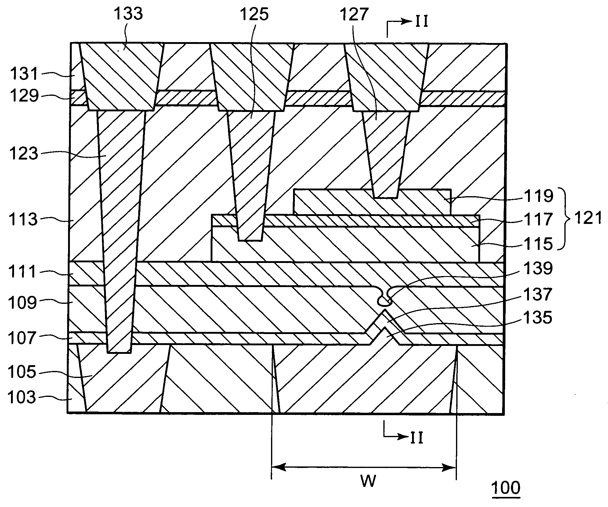
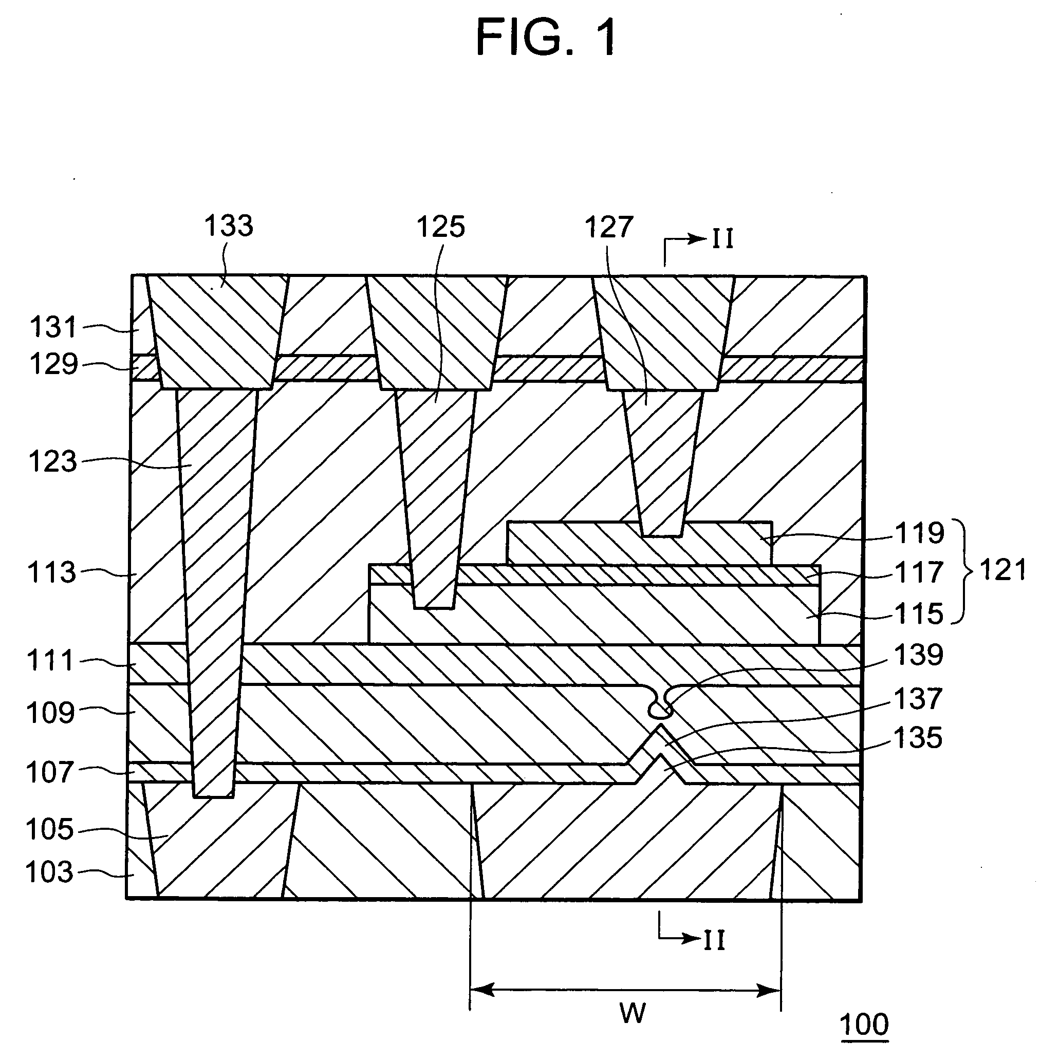
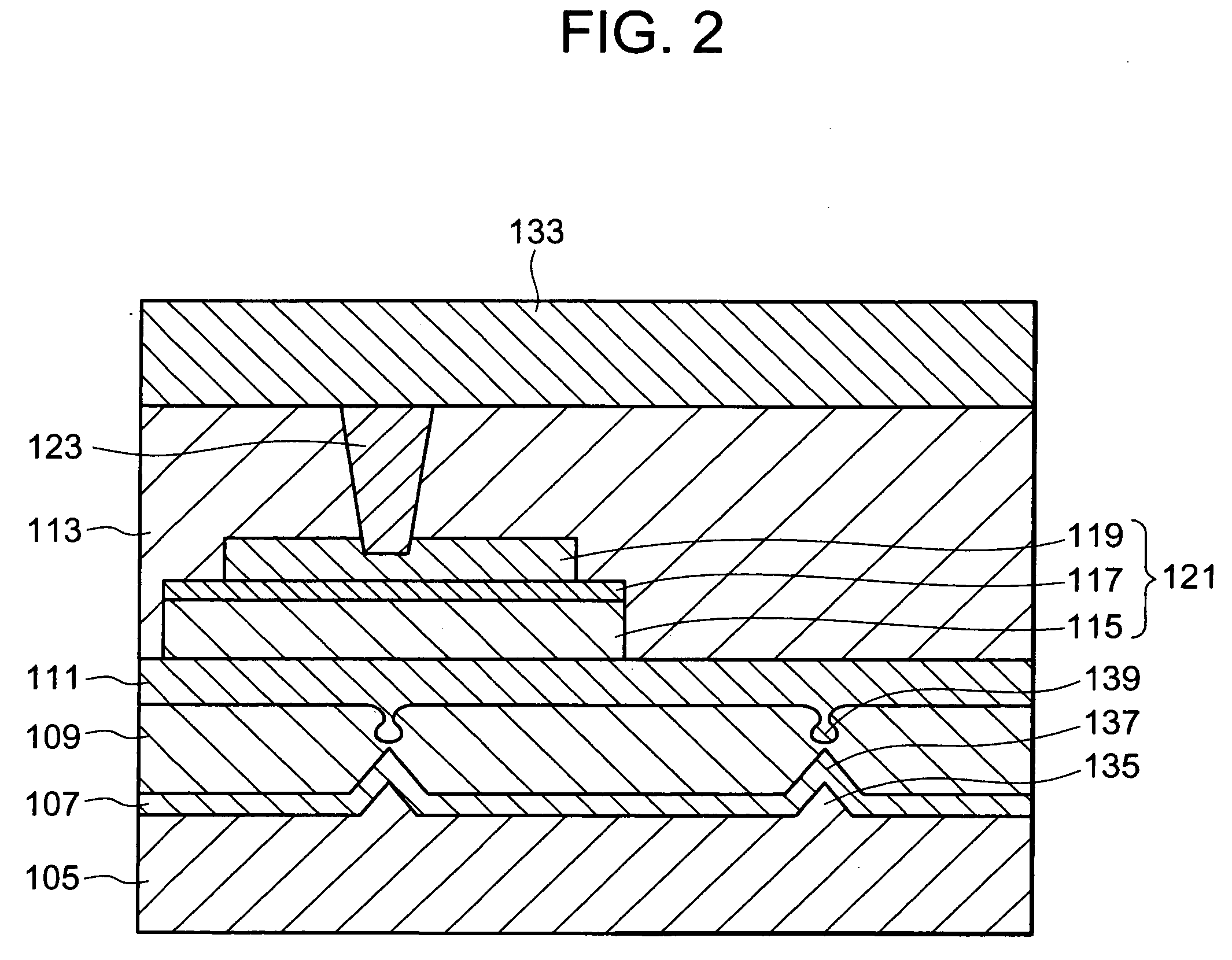
[0051]FIG. 1 is a cross-sectional view showing a structure of a semiconductor device according to an embodiment of the present invention. A semiconductor device 100 shown in FIG. 1 has a structure in which a first wiring layer (silicon oxide film (hereinafter, referred to as SiO2 film) 103 and first copper (Cu) wirings 105), a second insulating film (SiO2 film 109), a third insulating film (SiO2 film 111), and a capacitor element 121 are laminated above a semiconductor substrate such as a silicon substrate (not shown) in this order. A fourth insulating film (SiO2 film 113) covering the capacitor element 121 is provided on the SiO2 film 111. A second wirin...


PUM


Abstract

A semiconductor device includes a first wiring layer which is provided above a semiconductor substrate and includes a first insulating film and a wiring buried in the first insulating film, a second insulating film provided above the first wiring layer, a third insulating film provided on the second insulating film, and a capacitor element provided on the third insulating film. The wiring includes an upper surface having a protruding portion. The capacitor element includes a lower electrode provided on the third insulating film, a capacitor insulating film provided on the lower electrode, and an upper electrode provided on the capacitor insulating film.

Description

BACKGROUND OF THE INVENTION[0001]1. Field of the Invention[0002]The present invention relates to a semiconductor device and a method of manufacturing the semiconductor device. In particular, the present invention relates to a semiconductor device including a MIM element and a method of manufacturing the semiconductor device.[0003]2. Description of the Related Art[0004]Up to now, semiconductor devices including metal-insulator-metal (MIM) elements are described in JP 11-87650 A and JP 2007-49089 A.[0005]JP 11-87650 A describes a semiconductor chip including a memory cell array region and a peripheral circuit region. In the peripheral circuit region of the semiconductor chip, first wiring layers connected with impurity semiconductor regions are formed on an upper surface of an interlayer insulating film. Upper portions of the first wiring layers are covered with cap insulating films. A spin-on-glass (SOG) film is formed on the cap insulating films over the entire surface of a substrat...

Claims


Application Information

Patent Timeline
Patent Type & Authority Applications(United States)
IPC IPC(8): H01L29/92H01L21/02
CPCH01L28/40
Inventor FURUMIYA, MASAYUKITODA, TAKESHI
Owner RENESAS ELECTRONICS CORP
Why Eureka
Try Eureka