Light emission device and display device using the light emission device as a light source

a technology of light emission device and light source, which is applied in the direction of discharge tube luminescnet screen, discharge tube main electrode, instruments, etc., can solve the problems of low high-voltage stability of light emission device, difficult to improve the luminance of known light emission device, and limited effect of metal reflective layer for improving luminance, etc., to achieve the effect of suppressing arc discharge, improving high-voltage stability, and improving luminan

Inactive Publication Date: 2009-01-15
SAMSUNG SDI CO LTD
View PDF6 Cites 3 Cited by
  • Summary
  • Abstract
  • Description
  • Claims
  • Application Information

AI Technical Summary

Benefits of technology

[0013]Exemplary embodiments provide a light emission device having advantages of suppressing arc discharge by increasing high-voltage stability and of improving the luminance thereof by increasing an anode voltage and the reflection efficiency of a metal reflective layer, and a display device using the light emission device as its light source.
[0020]Some embodiments of a light emission device comprise a front substrate and a rear substrate sealed together at their peripheries. A light emission unit comprising a reflective layer, which is an anode, is disposed on an inside surface of the rear substrate, and a phosphor layer disposed on the reflective layer. Electron emission units comprising electron emission elements are disposed on an inside surface of the front substrate. Each electron emission element comprises a first electrode, a second electrode, and first electron emission regions disposed on either side of and coupled to the first electrode. Some embodiments also comprise second electron emission regions disposed on either side of and coupled to the second electrode. Electron emission regions are thinner than the corresponding electrode. Some embodiments permit application of higher anode voltages, thereby increasing the luminance of the device, while exhibiting reduced diode emission and arcing.

Problems solved by technology

As described above, the light emission device had low high-voltage stability and an upper limit to the anode voltage.
Therefore, it is difficult to improve the luminance of known light emission devices.
Furthermore, the effect of the metal reflective layer for improving luminance is limited in a structure in which electrons excite the phosphor layer after passing through the metal reflective layer, which then reflects visible light emitted toward the rear substrate, back to the front substrate.

Method used


Image

  • Light emission device and display device using the light emission device as a light source
  • Light emission device and display device using the light emission device as a light source
  • Light emission device and display device using the light emission device as a light source

Examples


Embodiment Construction

[0052]Certain embodiments will now be described more fully with reference to the accompanying drawings, in which exemplary embodiments are shown. The disclosure may, however, be embodied in many different forms and should not be construed as being limited to the embodiments set forth herein; rather these embodiments are provided so that this disclosure will be thorough and complete, and will fully convey the concepts thereof to those skilled in the art.

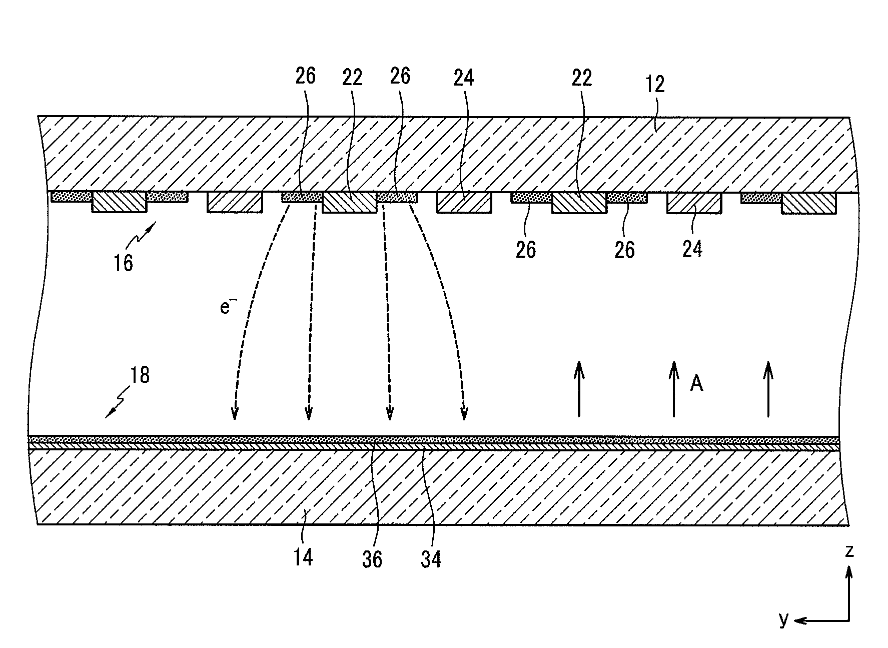
[0053]A light emission device 100 according to a first exemplary embodiment will be described with reference to FIGS. 1 to 3. In FIG. 3, the inner surface of a front substrate 12 is illustrated facing upward.

[0054]Referring to FIG. 1 to FIG. 3, a light emission device 100 of the present exemplary embodiment includes a front substrate 12 and a rear substrate 14 facing each other, generally in parallel, with a predetermined gap therebetween. The front and rear substrates 12 and 14 are sealed together along their peripheries with a seali...


PUM

PropertyMeasurementUnit
thickaaaaaaaaaa
thicknessaaaaaaaaaa
anode voltageaaaaaaaaaa

Abstract

A light emission device with improved high voltage stability, and a display device having the light emission device as its light source, the light emission device comprising front and rear substrates disposed to face each other, an electron emission unit disposed on the front substrate and having a plurality of electron emission elements, and a light emission unit including a metal reflective layer formed on the rear substrate and a phosphor layer formed on the metal reflective layer. Each of the electron emission elements includes first electrodes, second electrodes arranged between the first electrodes, and electron emission regions electrically connected to the first electrodes and having a thickness smaller that of the first electrodes.

Description

CROSS-REFERENCE TO RELATED APPLICATION[0001]This application claims priority to and the benefit of Korean Patent Application No. 10-2007-69606 filed in the Korean Intellectual Property Office on Jul. 11, 2007, the entire content of which is incorporated herein by reference.BACKGROUND[0002]1. Technical Field[0003]The present disclosure relates to a light emission device. More particularly, the present disclosure relates to a light emission device that improves the structures of an electron emission unit and a light emission unit, and a display device using the light emission device as a light source.[0004]2. Description of Related Art[0005]There are many different types of light emission devices that radiate visible light. One type of light emission device includes a structure in which an anode electrode and a phosphor layer are disposed on a front substrate and electron emission regions and driving electrodes are disposed on a rear substrate. The front and rear substrates are integr...

Claims


Application Information

Patent Timeline
Patent Type & Authority Applications(United States)
IPC IPC(8): H01J1/62
CPCG02F1/133602H01J63/06H01J63/02G02F1/1335H01J1/30
Inventor KIM, YOON-JINKIM, JAE-MYUNGJOO, KYU-NAMPARK, HYUN-KILEE, SO-RACHO, YOUNG-SUKMOON, HEE-SUNG
Owner SAMSUNG SDI CO LTD
Why Eureka
Try Eureka