Semiconductor memory device and method of generating chip enable signal thereof

a semiconductor memory and chip technology, applied in the field can solve the problems of complicated circuit configuration adversely affecting high-speed operation of semiconductor memory devices, etc., and achieve the effect of simple circuit configuration

Active Publication Date: 2009-01-15
SAMSUNG ELECTRONICS CO LTD
View PDF5 Cites 20 Cited by
  • Summary
  • Abstract
  • Description
  • Claims
  • Application Information

AI Technical Summary

Benefits of technology

[0013]An embodiment of the present invention provides a semiconductor memory device in which respective stacked

Problems solved by technology

However, since the counters CNT1 to CNTi of the memory chips 10-1 to 10-i are cascade-connected to one another, a next counter generates a delayed output value due to previous counters, thus adversely affecti

Method used


Image

  • Semiconductor memory device and method of generating chip enable signal thereof
  • Semiconductor memory device and method of generating chip enable signal thereof
  • Semiconductor memory device and method of generating chip enable signal thereof

Examples


Embodiment Construction

[0044]A semiconductor memory device and a method of generating a chip enable signal thereof according to the present invention will be described more fully hereinafter with reference to the accompanying drawings, in which exemplary embodiments of the invention are shown.

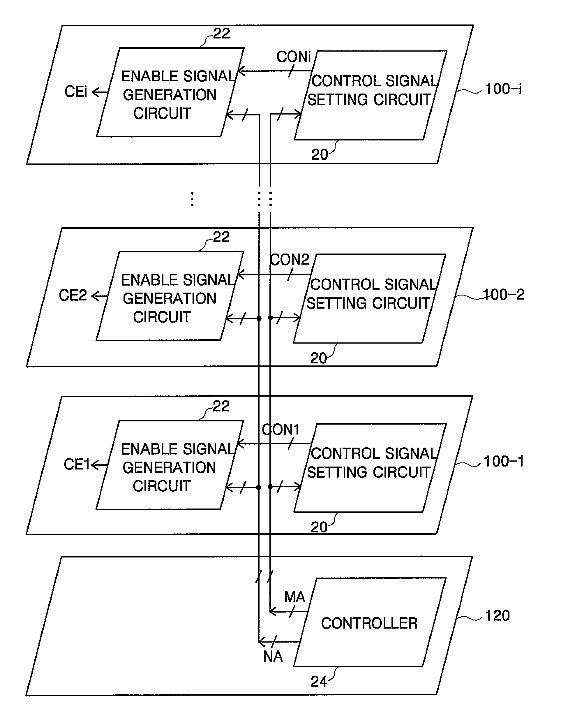
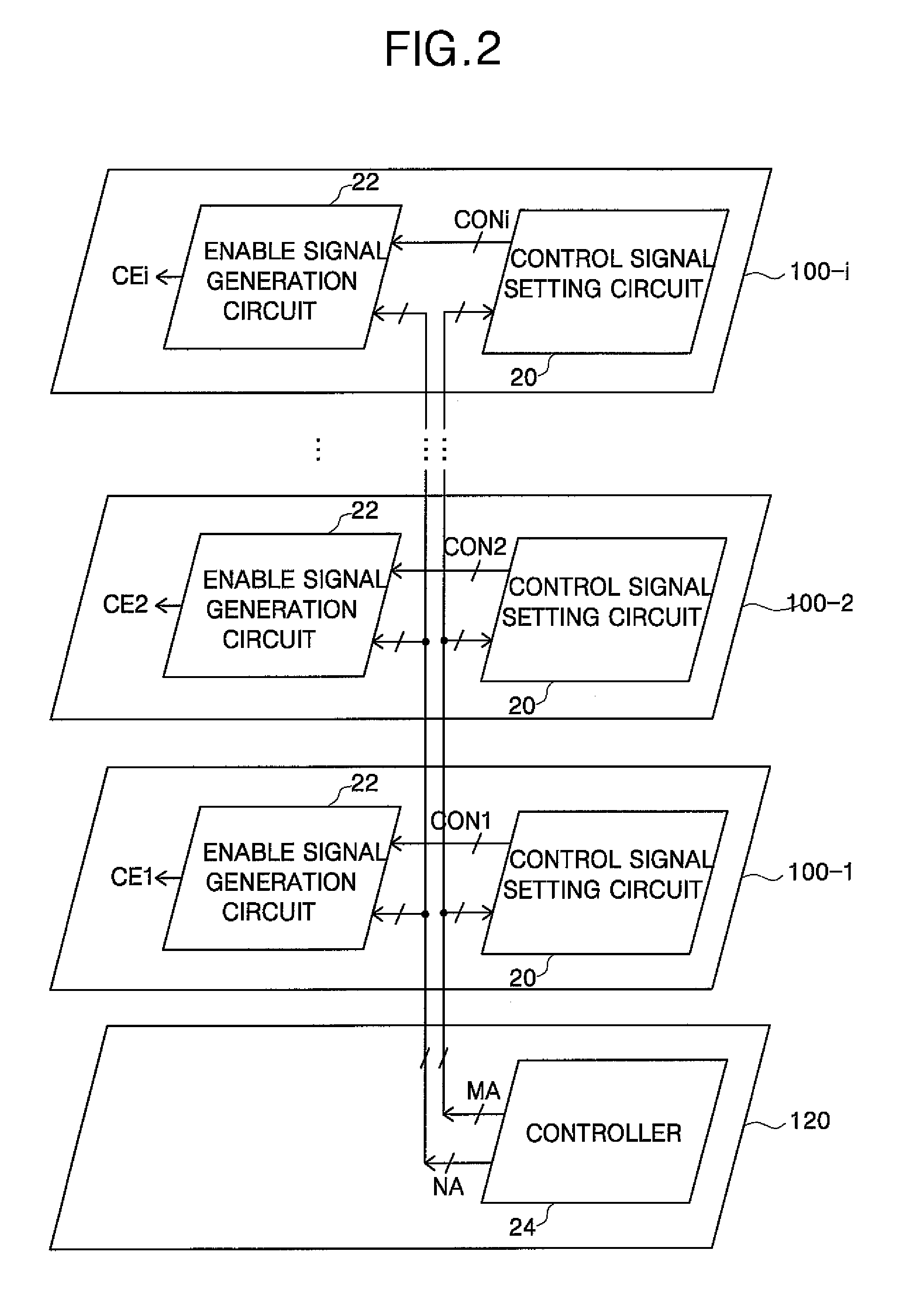
[0045]FIG. 2 is a diagram showing the configuration of a semiconductor memory device according to an exemplary embodiment of the present invention.

[0046]Referring to FIG. 2, the semiconductor memory device includes an i number of memory chips 100-1 to 100-i and an interface chip 120. Each of the memory chips 100-1 to 100-i includes a control signal setting circuit 20 and an enable signal generation circuit 22, and the interface chip 120 includes a controller 24.

[0047]Functions of the blocks shown in FIG. 2 will now be described.

[0048]The controller 24 generates a signal MA in response to an externally applied code signal, for example, an address signal applied through an address input terminal, during a mode register...


PUM


Abstract

Provided are a semiconductor memory device and a method of generating a chip enable signal thereof. The device includes a plurality of memory chips and an interface chip that are stacked. Each of the memory chips includes a control signal setting unit, which sets input signals applied to first and second input nodes as less significant 2-bit control signals of n-bit control signals, performs a logic AND operation on the less significant 2-bit control signals to generate AND operated signals, performs a logic XOR operation on each of the AND operated signals and each bit signal of more significant n−2-bit input signals applied to third to n-th input nodes to set the n−2-bit control signals, outputs the signal applied to the second input node through a first output node, inverts the signal applied to the first input node to output the inverted signal through a second output node, and outputs the more significant n−2-bit input signals through third through n-th output nodes, respectively. The first through n-th output nodes of one of two adjacent memory chips are respectively connected to the first through n-th input nodes of the other of the two adjacent memory chips.

Description

BACKGROUND OF THE INVENTION[0001]1. Field of the Invention[0002]The present invention relates to a semiconductor memory device and, more particularly, to a semiconductor memory device in which a plurality of chips are stacked and packaged and a method of generating a chip enable signal thereof.[0003]2. Description of Related Art[0004]In general, a semiconductor memory device is fabricated by packaging a single chip. Thus, both a memory portion for storing data and a control portion for controlling the input / output of data in / from the memory portion are integrated in the single chip.[0005]However, a semiconductor memory device packaged by stacking a plurality of chips has recently been introduced. In the semiconductor memory device, a control portion is provided in one of the chips, and a memory portion is provided in each of the remaining chips.[0006]In the semiconductor memory device in which the chips are stacked and packaged, each of the chips should include a chip enable signal ...

Claims


Application Information

Patent Timeline
IPC IPC(8): H03K19/21
CPCG11C7/1045H03K19/20G11C7/22G11C7/20
Inventor KIM, DOO-GONKIM, YOUN-CHEUL
Owner SAMSUNG ELECTRONICS CO LTD
Why Eureka
Try Eureka