Direct emulsion process for making printed circuits

a printing circuit and emulsion technology, applied in the field of printed circuit boards, can solve the problems of “loss” of high-speed rf applications, the prior art process requires several steps, and the limitations of imaging, development, and etching of fine lines

Inactive Publication Date: 2009-01-22
EARTHONE CIRCUIT TECH CORP +1
View PDF8 Cites 9 Cited by
  • Summary
  • Abstract
  • Description
  • Claims
  • Application Information

AI Technical Summary

Benefits of technology

[0006]The present invention is directed to a method for making printed circuits and printed circuit boards which eliminates the need for silver film used in imaging dry film in prior art processes. The method for making printed circuits and printed circuit boards in the present invention includes the steps of coating a non-metallized substrate with a solution which creates a l

Problems solved by technology

This prior art process requires several steps and has limitations on the imaging, developing, and etching of fine line images.
Imaging of much finer lines, for example imaging fine lines down to 0.0025 inches, creates a problem and is inconsistent w

Method used


Image

  • Direct emulsion process for making printed circuits
  • Direct emulsion process for making printed circuits
  • Direct emulsion process for making printed circuits

Examples


Embodiment Construction

[0018]Methods of the present invention for fabricating printed circuits and printed circuit boards generally include providing a non-metallized substrate, coating the non-metallized substrate, and imaging of a circuit design directly onto the coated substrate. The imaged substrate may then be developed with one or more chemistries and processed by subjecting it to an electroless solution in order to create a printed circuit or printed circuit board having a metal image. It should be understood by those skilled in the art that any type of non-metallized substrate may be used as long as the substrate is uniform for imaging. In addition, those skilled in the art will understand that a number of photosensitive chemicals may be used to coat the surface of the non-metallized substrate and that a variety of chemistries may be used to develop the imaged substrate.

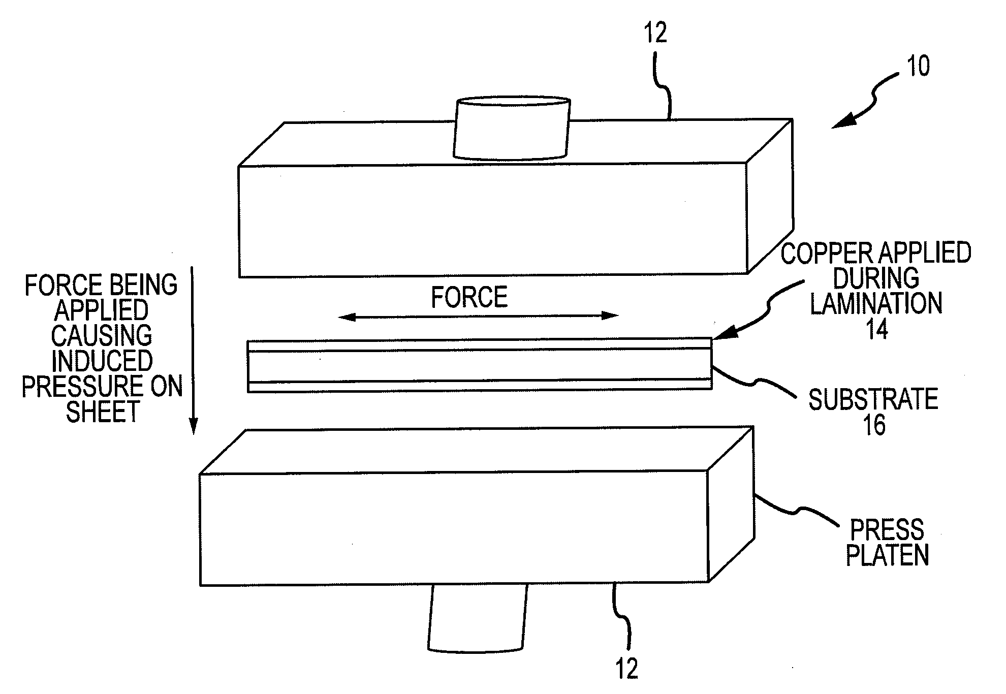
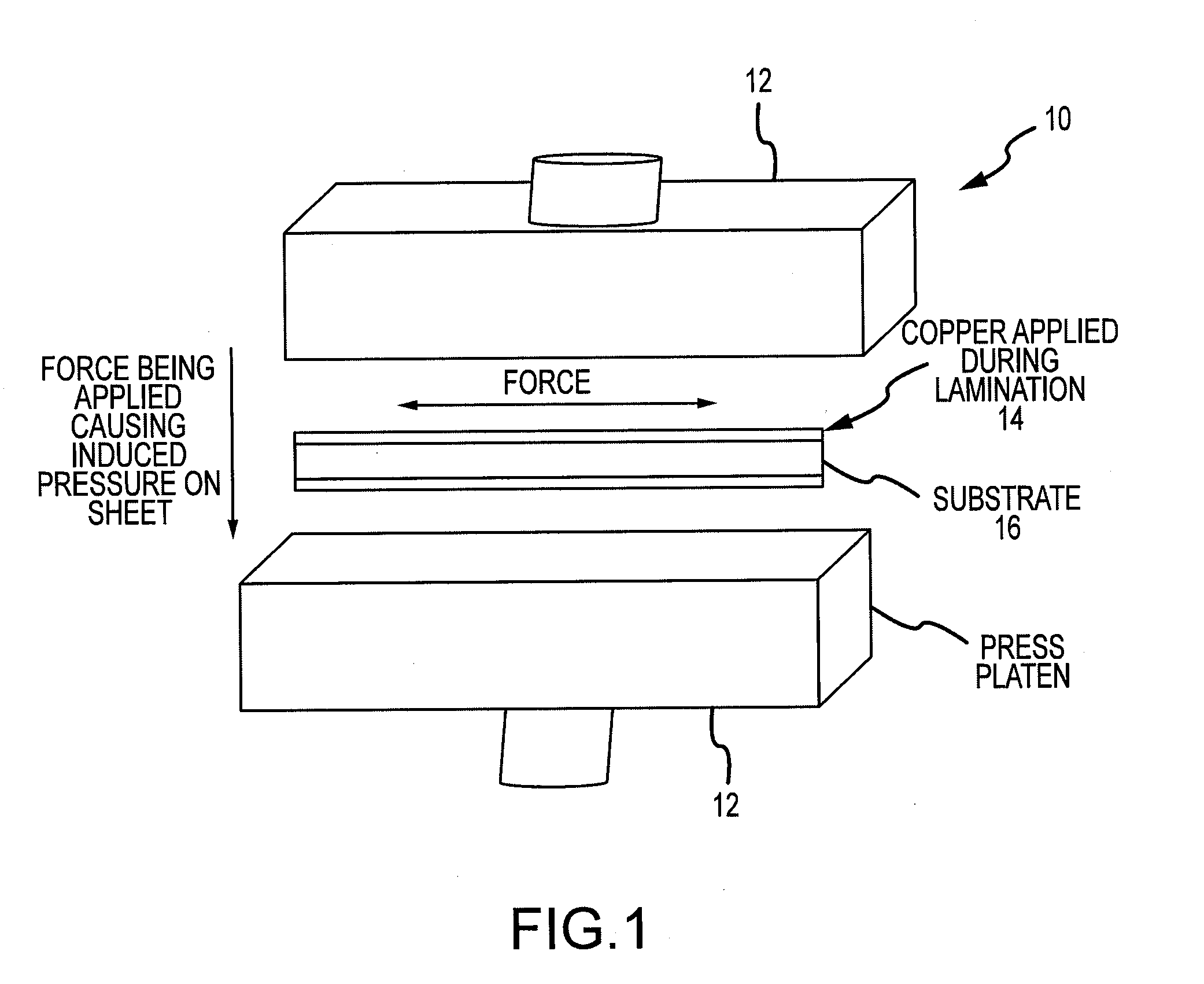
[0019]FIG. 1 is a schematic showing the prior art conventional process 10 for laminating copper to a substrate. A large laminatio...


PUM

PropertyMeasurementUnit
Lengthaaaaaaaaaa
Temperatureaaaaaaaaaa
Sensitivityaaaaaaaaaa

Abstract

A direct emulsion process for making printed circuits and printed circuit boards which includes coating a non-metallized substrate with a solution which creates a light sensitive surface on the substrate, imaging the coated substrate with a circuit design, developing the imaged substrate, and directly plating the developed image onto the coated substrate. Coating solutions which work particularly well in this process include a ferric oxalate and palladium emulsion or a silver based emulsion.

Description

CROSS-REFERENCE TO RELATED APPLICATIONS[0001]This patent application is a continuation-in-part of patent application having Ser. No. 11 / 751,350, filed May 21, 2007, and also claims priority to U.S. provisional patent application having Ser. No. 60 / 944,715 filed Jun. 18, 2007, both of which are herein incorporated in their entireties.FIELD OF INVENTION[0002]The present invention relates to a printed circuit board technology and more particularly to a direct emulsion process for making printed circuits which includes coating a non-metallized substrate with a solution which creates a light sensitive surface on the substrate, imaging the coated substrate with a circuit design, developing the imaged substrate, and directly plating the developed image onto the coated substrate. The present invention also relates to printed circuits and printed circuit boards which result from this method.BACKGROUND OF THE INVENTION[0003]Prior art processes for making printed circuits and printed circuit b...

Claims


Application Information

Patent Timeline
IPC IPC(8): G03F7/20H05K1/09H05K3/10
CPCH05K3/106Y10T29/49155H05K2203/107H05K3/185
Inventor DUTTON, STEVEN LEE
Owner EARTHONE CIRCUIT TECH CORP
Why Eureka
Try Eureka