


Quick Research
Generate reliable direction feasibility study reports for your R&D in just a few steps.

Technical Q&A
Discover and master advanced knowledge NOW. Basics, ideas, possibilities, all at once.

Find Solutions
As an expert in R&D theories, this can generate solutions to your technical problems instantly.

Evaluate Feasibility
Analyze your overall solution with one click, know your potential R&D risks in advance.

Monitor Landscape
Get weekly tech updates, stay abreast of the latest tech innovations and key insights.
Semiconductor switching device
a switching device and semiconductor technology, applied in the direction of electronic switching, semiconductor devices, pulse techniques, etc., can solve the problem of reducing the switching tim
- Summary
- Abstract
- Description
- Claims
- Application Information
AI Technical Summary
Problems solved by technology
Method used
Image

Examples
first embodiment
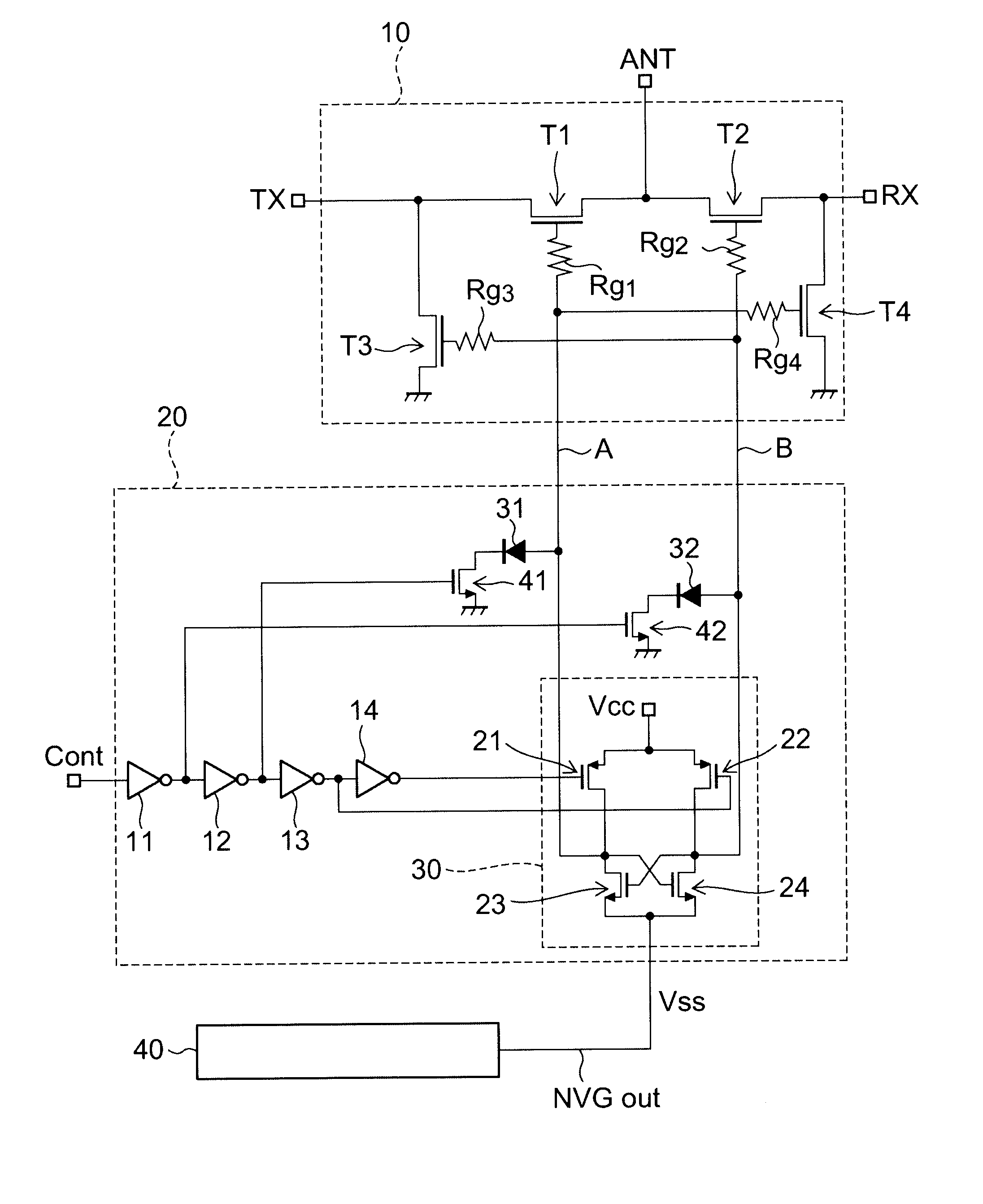
[0025]FIG. 1 is a circuit diagram of a high-frequency semiconductor switching device according to a first embodiment of the invention.
[0026]The high-frequency semiconductor switching device according to this embodiment comprises, on the same semiconductor substrate (semiconductor chip), a high-frequency switching circuit 10 for switching the connection states between a plurality of terminals, a negative voltage generating circuit 40, and a control circuit 20 connected to the high-frequency switching circuit 10 and the negative voltage generating circuit 40 and configured to supply a control signal to the high-frequency switching circuit 10.
[0027]The high-frequency switching circuit 10 includes four FETs (field effect transistors). A through transistor T1 is connected between a transmitting terminal TX and an antenna terminal ANT. A through transistor T2 is connected between a receiving terminal RX and the antenna terminal ANT. A shunt transistor T3 is connected between the transmitt...
second embodiment
[0078]FIG. 4 is a circuit diagram of a high-frequency semiconductor switching device according to a second embodiment of the invention.
[0079]In this embodiment, the configuration of the level shift circuit 130 is different from that of the above first embodiment. More specifically, between the drain of the pair of PMOSs 21, 22 and the pair of complementary output terminals (output nodes A, B), a pair of PMOSs 25, 26 are additionally placed with each gate connected to the ground. Furthermore, between the drain of the pair of NMOSs 23, 24 and the pair of complementary output terminals (output nodes A, B), a pair of NMOSs 27, 28 are additionally placed with each gate supplied with a certain potential Vbias. By cascode connection between the pair of PMOSs 25, 26 and the pair of NMOSs 27, 28, the voltage applied between the electrodes of each MOS is limited to prevent the voltage between any pair of electrodes of each MOS from exceeding the breakdown voltage.
[0080]In the level shift circ...
third embodiment
[0081]FIG. 5 is a block diagram showing the configuration of a high-frequency semiconductor switching device according to a third embodiment of the invention.
[0082]The high-frequency multiport switching circuit 52 corresponds to the high-frequency switching circuit 10 in FIG. 1. The high-frequency multiport switching circuit 52 includes one antenna terminal ANT and X high-frequency terminals RF1-RFX. Each high-frequency terminal RF1-RFX corresponds to the transmitting terminal TX or the receiving terminal RX.
[0083]A plurality of control circuits 20 are connected to the high-frequency multiport switching circuit 52. Each control circuit 20 corresponds to the control circuit 20 shown in FIG. 1 or 4. A negative voltage generating circuit 40 is connected to the low-potential power supply terminal of the level shift circuit in each control circuit 20.
[0084]Each control circuit 20 is connected to a decoder circuit 51. The decoder circuit 51 is an M / N decoder circuit, which decodes control...
PUM
 Abstract
Description
Claims
Application Information
 - R&D Engineer
- R&D Manager
- IP Professional
- Industry Leading Data Capabilities
- Powerful AI technology
- Patent DNA Extraction
Browse by: Latest US Patents, China's latest patents, Technical Efficacy Thesaurus, Application Domain, Technology Topic, Popular Technical Reports.
© 2024 PatSnap. All rights reserved.Legal|Privacy policy|Modern Slavery Act Transparency Statement|Sitemap|About US| Contact US: help@patsnap.com