Eureka AIR delivers breakthrough ideas for toughest innovation challenges, trusted by R&D personnel around the world.

Circuit board structure with concave conductive cylinders and method for fabricating the same

Inactive Publication Date: 2009-01-29
UNIMICRON TECH CORP
View PDF3 Cites 3 Cited by
  • Summary
  • Abstract
  • Description
  • Claims
  • Application Information

AI Technical Summary

Benefits of technology

[0008]The present invention provides a circuit board structure with concave conductive cylinders and the fabricating method thereof, for fabricating circuit board structure with concave conductive cylinders, so that the bonding quality between solder material and conductive cylinder is better.
[0009]The present invention provides a fabricating method of circuit board structure with concaved conductive cylinders. The method includes: providing a conductive layer first; forming a plurality of conductive cylinders on a surface of the conductive layer; forming a dielectric layer on the surface of the conductive layer on which the conductive cylinders are formed; exposing the tips of these conductive cylinders out of a surface of the dielectric layer relatively far away from the conductive layer; removing the tips of the conductive cylinders, so that the height of the conductive cylinders is lower than the height of the dielectric layer and the conductive cylinders sunk into the dielectric layer.
[0023]Since the present invention forms the dielectric layer on the outside of the conductive layer, to substitute the function of solder mask layer, therefore the solder mask opening drift problem occurred in the prior arts because the solder mask layer has to align with the pads, or the problem that the solder mask openings are too small when image transfers can be avoided. In addition, since the conductive cylinders are sunk into the dielectric layer, so that the solder material can be filled in the dielectric layer and to effectively bond to the conductive cylinders, therefore the bonding reliability of the solder material and the conductive cylinders can be improved, and disposing pads is no more required.

Problems solved by technology

In addition, when an image transfers, light leaking, under exposure, less developing power or incomplete development may also lead to too small openings 132.

Method used


Image

  • Circuit board structure with concave conductive cylinders and method for fabricating the same
  • Circuit board structure with concave conductive cylinders and method for fabricating the same
  • Circuit board structure with concave conductive cylinders and method for fabricating the same

Examples


first embodiment

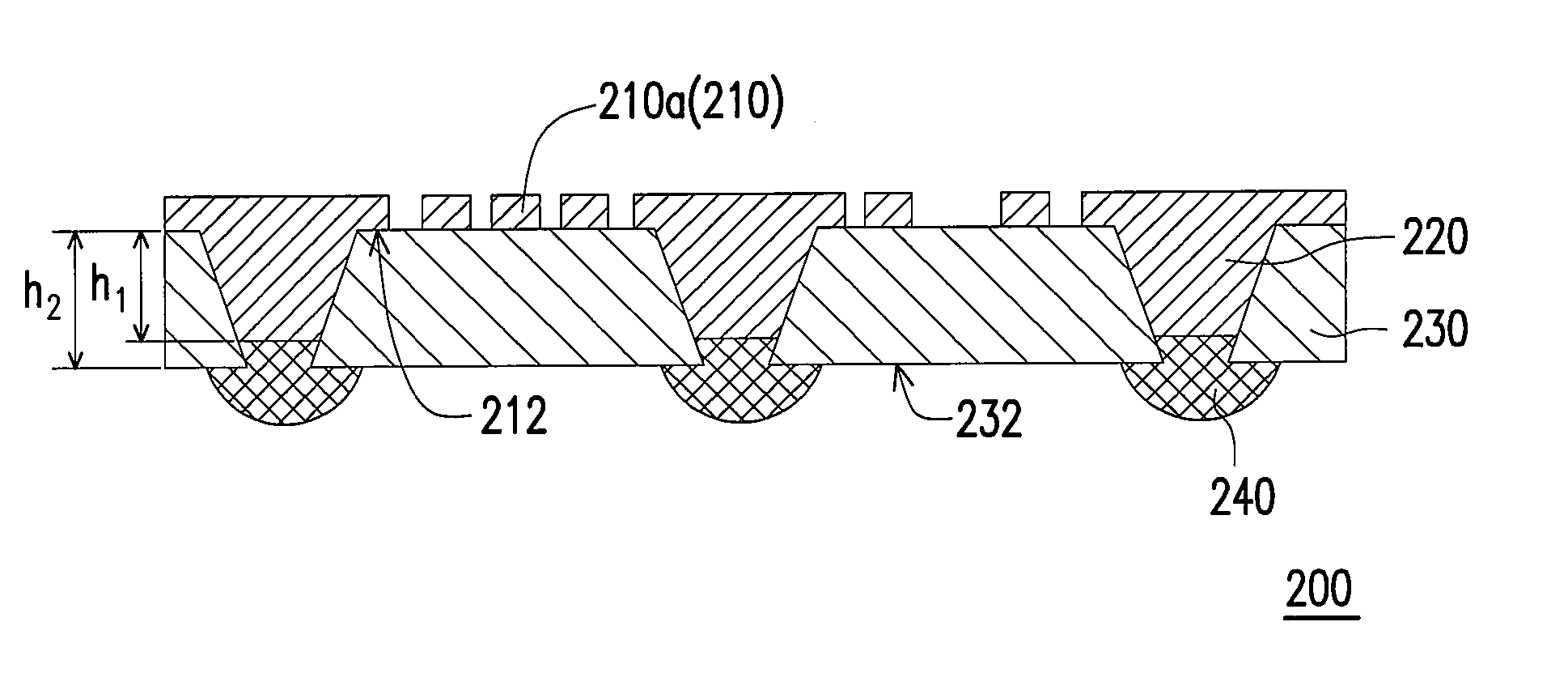
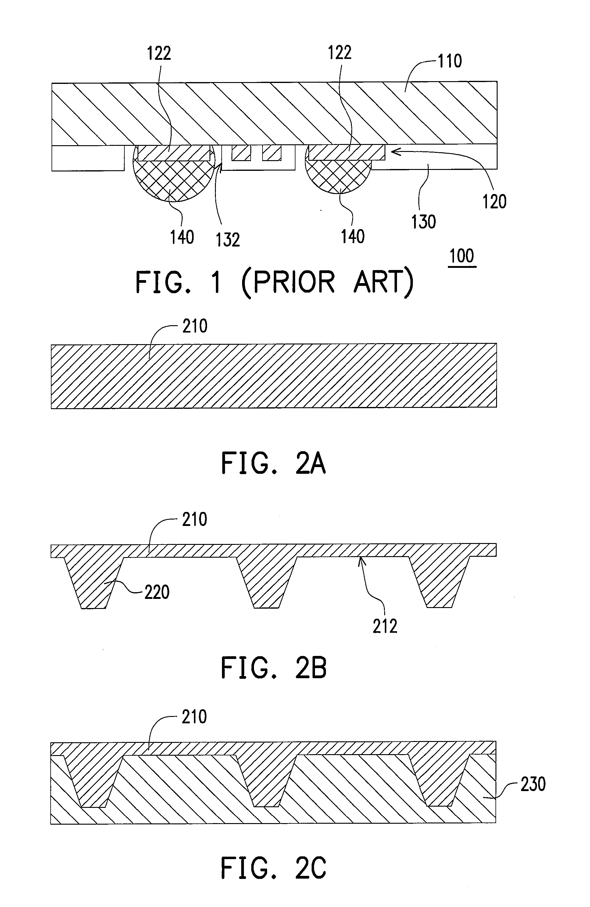
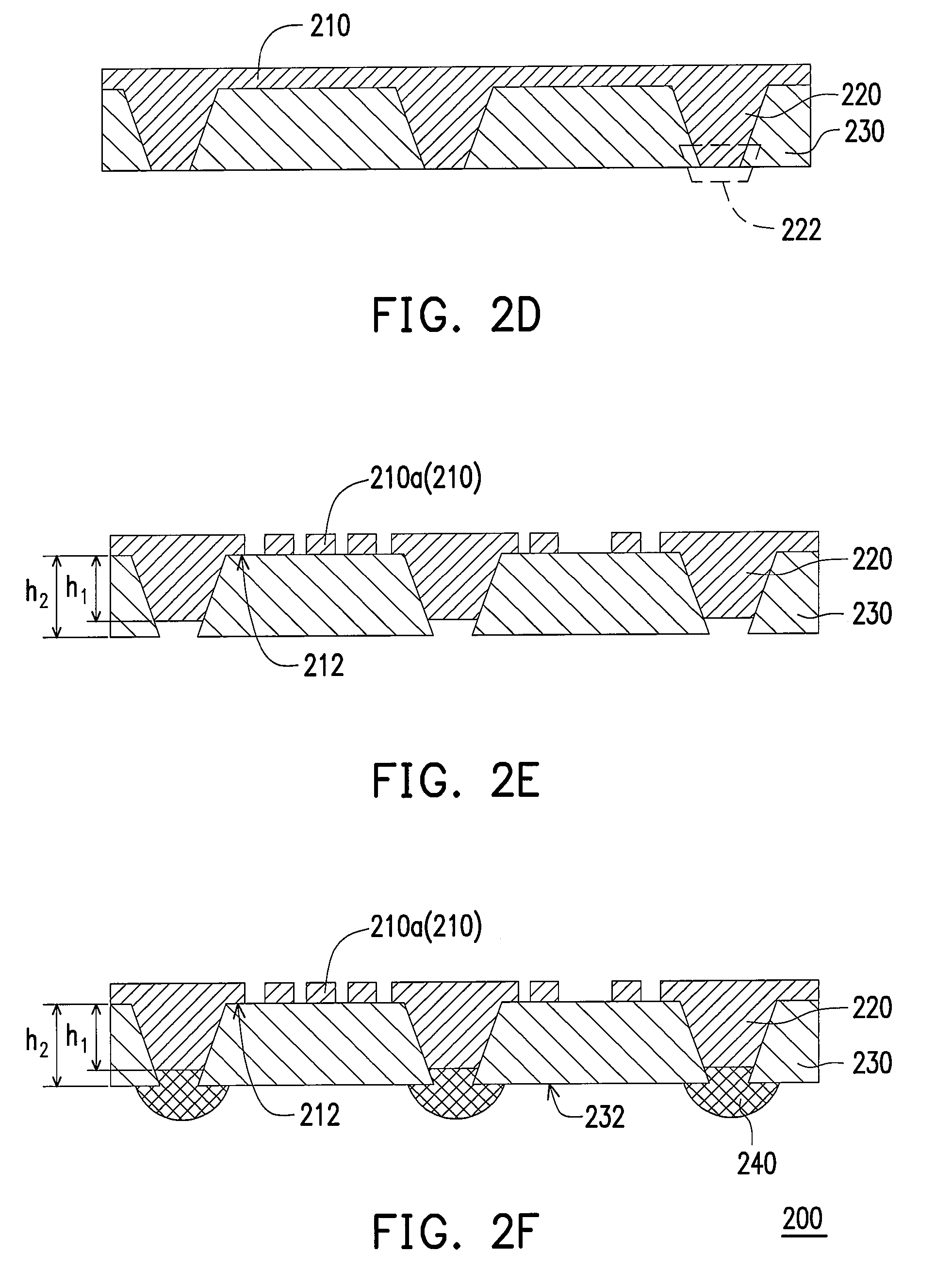
[0028]FIG. 2A˜FIG. 2F are flow diagrams of fabricating the circuit board structure with concave conductive cylinders of the first embodiment of the present invention. With reference to FIG. 2A, first a conductive layer 210 is provided, the conductive layer 210 for example is a metal layer, the material of the conductive layer 210 may be copper. Next, with reference to FIG. 2B, partially etching the conductive layer 210 is conducted, so that a plurality of conductive cylinders 220 are formed on the surface 212 of the conductive layer. In another embodiment which is not shown, the conductive cylinders 220 may also be formed on the surface 212 of the conductive layer 210 through forming bumps using welding wire machine or through other appropriate method.

[0029]Next, with reference to FIG. 2C, a dielectric layer 230 is formed on the surface 212 of the conductive layer 210 on which the conductive cylinders 220 are formed. The method of forming the dielectric layer 230 on the conductive l...

second embodiment

[0034]FIG. 3A˜FIG. 3F are diagrams of the flow of fabricating the circuit board structure with concave conductive cylinders of the second embodiment of the present invention. The present embodiment is similar to the previous embodiment, the only difference is that: in the previous embodiment, the dielectric layer 230 is formed after the conductive cylinders 220 are formed; while in the present embodiment, the dielectric layer 320 is formed before the conductive cylinders 330 are formed. Refer the following descriptions for the flow detail, the similarities thereof will not be repeated.

[0035]With reference to FIG. 3A, a conductive layer 310 which has a surface 312 is formed. Next, with reference to FIG. 3B, by using laminating method or printing method or the alike, a dielectric layer 320 is formed on the surface 312 of the conductive layer 310 on which the conductive cylinders 330 are formed. Further next, with reference to FIG. 3C, a plurality of vias 322 are formed in the dielectr...


PUM

PropertyMeasurementUnit
Electrical conductoraaaaaaaaaa
Heightaaaaaaaaaa

Abstract

A method for fabricating a circuit board structure with concave conductive cylinders is provided. Firstly, a conductive layer is provided; a plurality of conductive cylinders are formed on a surface of the conductive layer; a dielectric layer is formed on the surface of the conductive layer with the conductive cylinders; the tips of the conductive cylinders are exposed on a surface of the dielectric layer far away from the conductive layer; removing the exposed tips of the conductive cylinders such that the height of the conductive cylinders is lower than the height of the dielectric layer, and the conductive cylinders sunk into the dielectric layer.

Description

CROSS-REFERENCE TO RELATED APPLICATION[0001]This application claims the priority benefit of Taiwan application serial no. 96127050, filed on Jul. 25, 2007. All disclosure of the Taiwan application is incorporated herein by reference.BACKGROUND OF THE INVENTION[0002]1. Field of the Invention[0003]The present invention relates to a circuit board structure and the fabricating method thereof, more specifically, the present invention relates to a circuit board structure with concave conductive cylinders and the fabricating method thereof.[0004]2. Description of Related Art[0005]Generally, conventional circuit boards used to carry and electrically connect a plurality of electronic elements are mainly formed with a plurality of interlayered patterned conductive layers and dielectric layers. The patterned conductive layers are defined and formed through patterning copper foil directly, or through copper electroplating upon copper foil to increase the thickness of conductive layer and then g...

Claims


Application Information

Patent Timeline
IPC IPC(8): H05K3/00
CPCH01L21/486H01L23/5384H01L23/49816H05K2201/09472H05K3/423Y10T29/49126H05K2203/0733H05K2201/09827H05K3/4647H01L2924/0002Y10T29/49124Y10T29/49155Y10T29/49165H01L21/4853Y10T29/49128H05K3/06H05K1/113H05K2201/0394H05K3/3457H01L2924/00H01K3/10
Inventor LEE, SHAO-CHIENCHANG, CHIH-MING
Owner UNIMICRON TECH CORP
Why Eureka
Eureka Blog
Learn More