Eureka AIR delivers breakthrough ideas for toughest innovation challenges, trusted by R&D personnel around the world.

Package substrate structure and bonding method thereof

a substrate structure and packaging technology, applied in the field of packaging techniques, can solve the problems of poor manufacturing yield, complex manufacturing process, and inability to reduce manufacturing costs, and achieve the effects of favorable bonding strength and bonding quality, and low temperature bonding

Active Publication Date: 2020-02-06
UNIMICRON TECH CORP
View PDF0 Cites 1 Cited by
  • Summary
  • Abstract
  • Description
  • Claims
  • Application Information

AI Technical Summary

Benefits of technology

The invention provides a package substrate structure and a bonding method that can be done at low temperatures and has strong bonding strength and quality. This reduces the process requirements, manufacturing cost, and improves manufacturing yield and quality of the package substrate structure. A macromolecular adhesive layer can be added to improve bonding with the first substrate. The conductive pillars fill in the gaps between the substrates and provide favorable electrical connection with the pads. Overall, this invention solves the problem of warping on substrate material, improves the manufacturing process of package substrate structures, and improves the quality, reliability, and electrical properties of the structure.

Problems solved by technology

In addition, because the surface of the copper structure needs to be well cleaned for obtaining a flat surface through a chemical polishing process (CMP) before bonding, the manufacturing process is complicated so manufacturing cost cannot be reduced.
In addition, an asymmetric structure produced when the fine circuit is formed on a substrate may lead to a problem of warpage on substrate material, which would result in poor manufacturing yield.

Method used


Image

  • Package substrate structure and bonding method thereof
  • Package substrate structure and bonding method thereof
  • Package substrate structure and bonding method thereof

Examples


Embodiment Construction

[0033]Some embodiments are provided hereinafter and described in detail with reference to the accompanied drawings. However, the embodiments provided are not intended to limit the scope of the invention. Further, the drawings are only descriptive and are not drawn to scale. For ease of explanation, the same devices below are provided with the same reference numerals.

[0034]Moreover, terms such as “first” and “second” used herein do not represent sequence or order, and it should be understood that they are only for differentiating devices or operations having the same technical terms.

[0035]Furthermore, terms such as “contain”, “include”, and “have” used herein are all open terms, i.e., contains, but not limited to.

[0036]In addition, terms such as “contacted”, “connected”, and “bonded” used herein refer to a direction contact or indirect contact through other film layers unless otherwise stated.

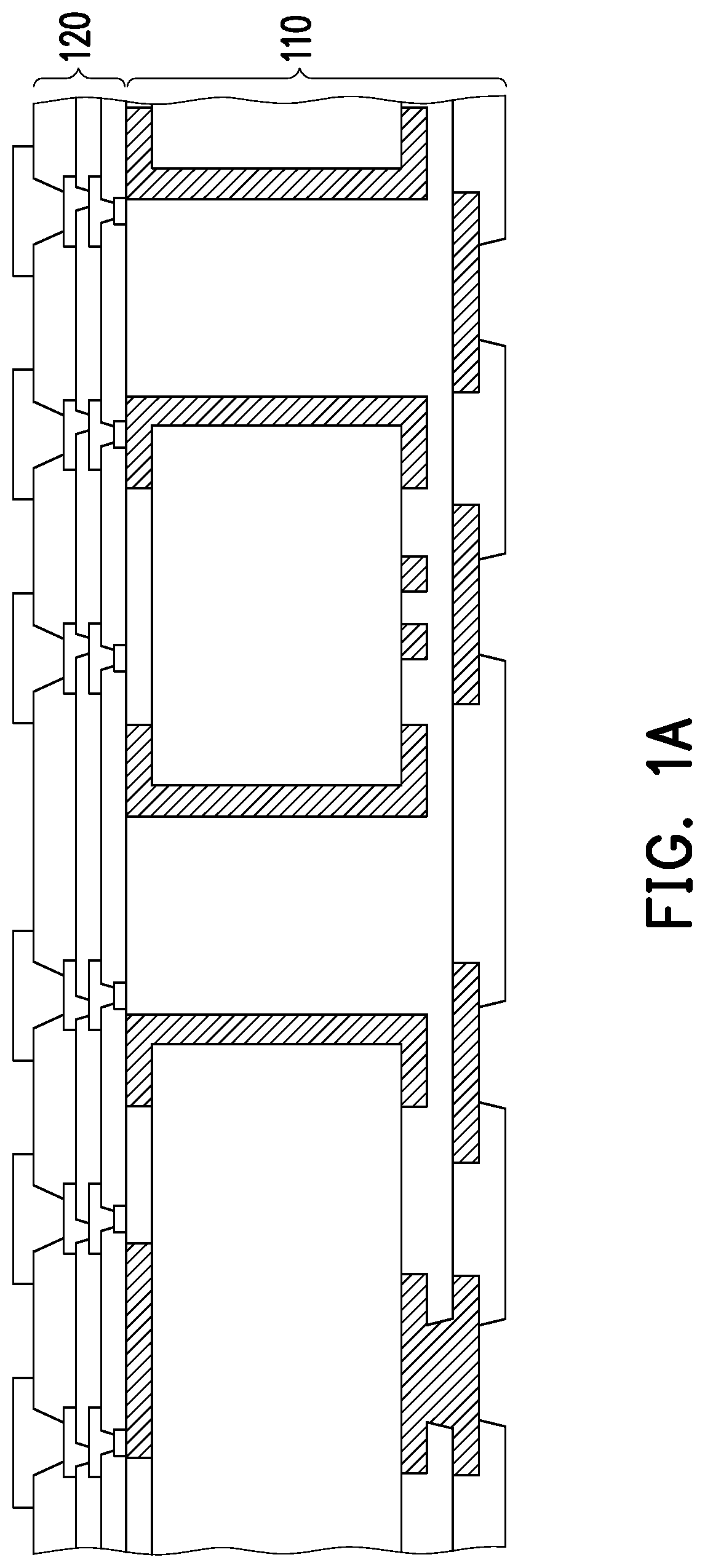
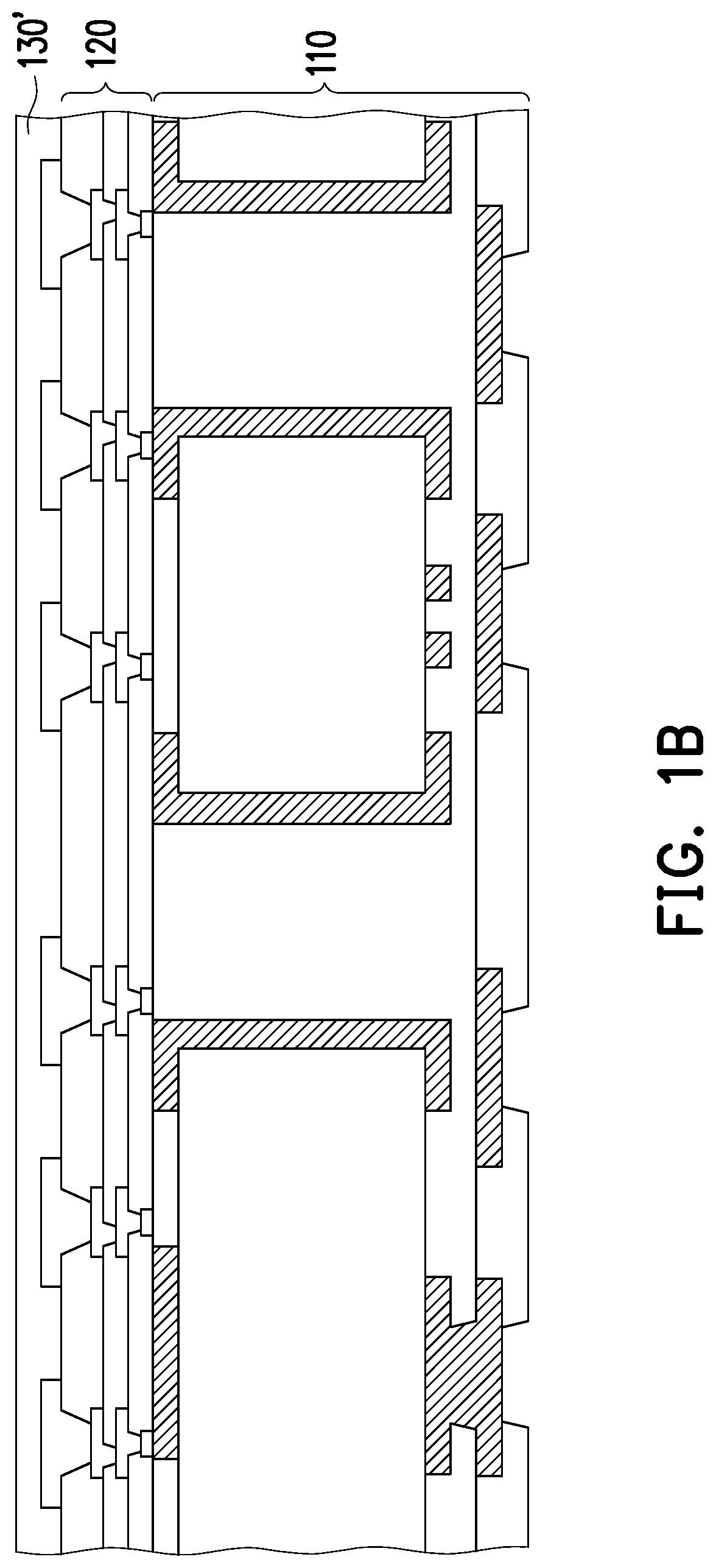
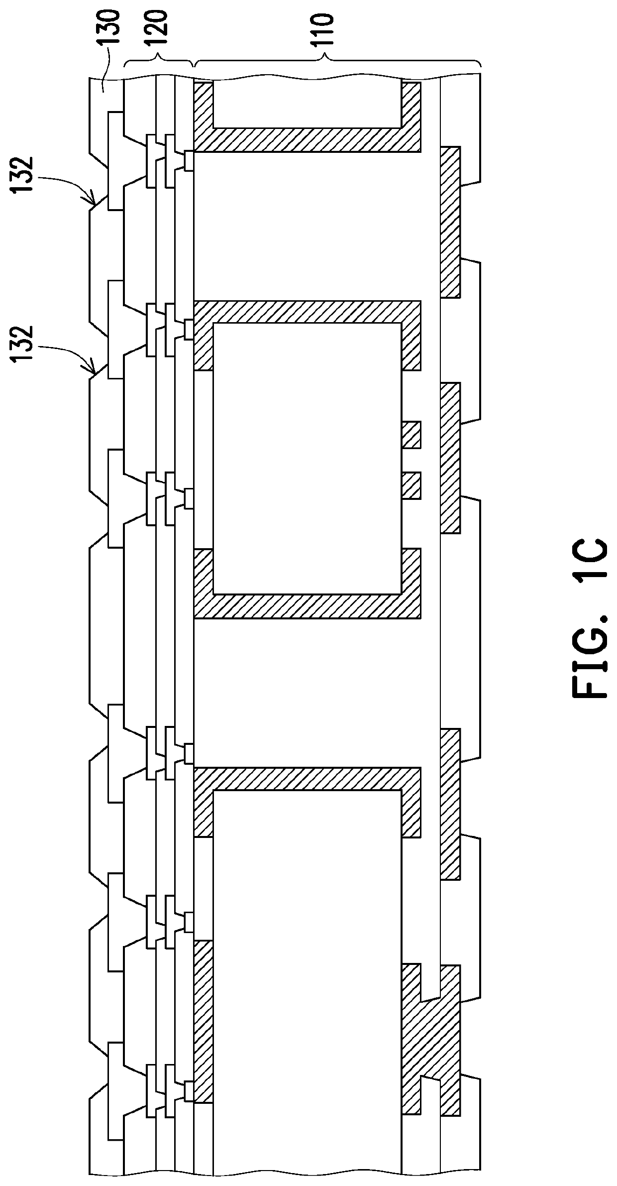
[0037]FIG. 1A to FIG. 1H are cross-sectional views illustrating a manufacturing process of a...


PUM


Abstract

A package substrate structure includes a first substrate, a second substrate, a plurality of conductive pillars and an adhesive layer. The first substrate includes a plurality of vias and a plurality of pads. The vias and the pads are disposed on the first substrate, and fills in the vias. The second substrate is disposed opposite to the first substrate. Each conductive pillar is disposed between the first substrate and the second substrate, where each conductive pillar electrically connects each pad and the second substrate, and the adhesive layer fills in the gaps between the conductive pillars. A bonding method of the package substrate structure is also provided.

Description

CROSS REFERENCE TO RELATED APPLICATION[0001]This application claims the priority benefit of Taiwan application serial no. 107127116, filed on Aug. 3, 2018. The entirety of the above-mentioned patent application is hereby incorporated by reference herein and made a part of specification.BACKGROUNDTechnical Field[0002]The invention relates to a packaging technique, and more particularly, to a package substrate structure and a bonding method of a package substrate structure.Description of Related Art[0003]With the evolution of semiconductor packaging technology, different package types have been developed for semiconductor devices, such as wire bonding, flip chip or hybrid (i.e., flip chip together with wire bonding) packaging techniques. In the pursuit of high efficiency and downsized package volume, as volume of fine circuit becomes more refined, the resistance value would also increase more to further reduce performance.[0004]Currently, there are packaging technologies that use a co...

Claims


Application Information

Patent Timeline
IPC IPC(8): H01L23/498
CPCH01L23/49838H01L2224/04H01L23/49833H01L23/49822H01L21/4857H01L23/145
Inventor KO, CHENG-TAYANG, KAI-MINGCHEN, YU-HUATSENG, TZYY-JANG
Owner UNIMICRON TECH CORP
Why Eureka
Eureka Blog
Learn More