Processing method

a multi-chamber type, processing method technology, applied in plasma technique, electrostatic charge, chemical/physical/physicochemical processes, etc., can solve the problems of deteriorating throughput increasing the difficulty of processing, and affecting the efficiency of multi-chamber-type processing apparatus. , to achieve the effect of preventing the ill effects of electric charge, reducing the difficulty of processing, and reliably removing a charg

Inactive Publication Date: 2009-01-29
TOKYO ELECTRON LTD
View PDF7 Cites 10 Cited by
  • Summary
  • Abstract
  • Description
  • Claims
  • Application Information

AI Technical Summary

Benefits of technology

[0009]It is, therefore, an object of the present invention to provide a multichamber-type processing apparatus and a processing method using same, which reliably neutralizes a charge on a substrate without incurring damage to the substrate, thereby ensuring excellent accuracy and throughput.
[0014]In the present invention, N was employed, however, there are elements such as F, O, and Cl that have the electronegativity greater than or equivalent to that of N. Since, however, F reacts with SiO2 formed on the substrate; O reacts with a resist; and Cl reacts with Si, N is preferred over F, O, and Cl. Furthermore, N is a non-toxic, non-explosive, incombustible, and relatively cheap substance. Moreover, its treatment is relatively easy, which makes N more of a preferred choice over the other elements.
[0016]Additionally, a charge on a substrate supporting unit of a transfer mechanism or on the substrate mounted thereon may be removed by supplying the dissociated monatomic N atoms into the transfer chamber, thereby further preventing ill effects of electric charge.
[0017]Furthermore, a charge on the substrate is removed at a desired time by controlling a supply timing of the dissociated monatomic N atoms, to effectively remove charge on the substrate.
[0018]Moreover, the energy supply unit may include an ultraviolet irradiation unit for irradiating ultraviolet ray to the N2 gas. In addition, a portion of a pipe may be made of a dielectric material, and an induction coil as the energy supply unit may be wound around the dielectric portion of the pipe, wherein a high frequency source applies a high frequency to the induction coil. As a result, the dissociated monatomic N atoms are conveniently obtained.
[0019]Furthermore, the dissociated monatomic N atoms may be effectively generated by applying energy, higher than dissociation energy of the N2 gas and lower than ionization energy of the N2 gas, to the N2 gas. When the energy applied to the N2 gas is lower than the dissociation energy, the N2 gas is not dissociated into the monatomic N atoms. On the other hand, when the energy applied to the N2 gas is higher than the ionization energy, more N ions are generated than the dissociated monatomic N atoms, which damages the substrate.

Problems solved by technology

The electric charge remaining on a surface of the substrate in the multichamber-type processing apparatus becomes an issue when transferring a substrate from a processing chamber to another processing chamber by use of the transfer arm.
Additionally, such condition also suffers from that it takes a relatively longer amount of time to separate the substrate from the electrostatic chuck, which in turn deteriorates throughput efficiency of the multichamber-type processing apparatus.
However, there are drawbacks associated with the method disclosed in Japanese Patent Laid-open Publication No. 1997-213780.
In such method, it is difficult to apply the current to the substrate so as to precisely neutralize the electric charge, and thus either positive or negative electric charge still remains on a surface of the substrate when a desired valance is not obtained, reducing neutralization of the substrate.
Furthermore, in case of employing the process disclosed in Japanese Patent Laid-open Publication No. 1994-275546 there is a concern for damages incurring on the substrate such as the semiconductor wafer, by the ionized processing gas supplied thereto.

Method used


Image

  • Processing method
  • Processing method
  • Processing method

Examples


Embodiment Construction

[0028]Hereinafter, the preferred embodiments of the present invention will now be described in reference to the accompanying drawings.

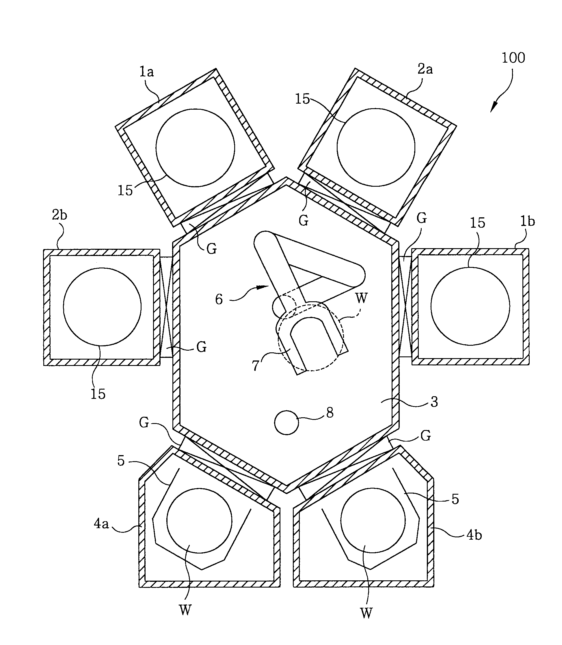
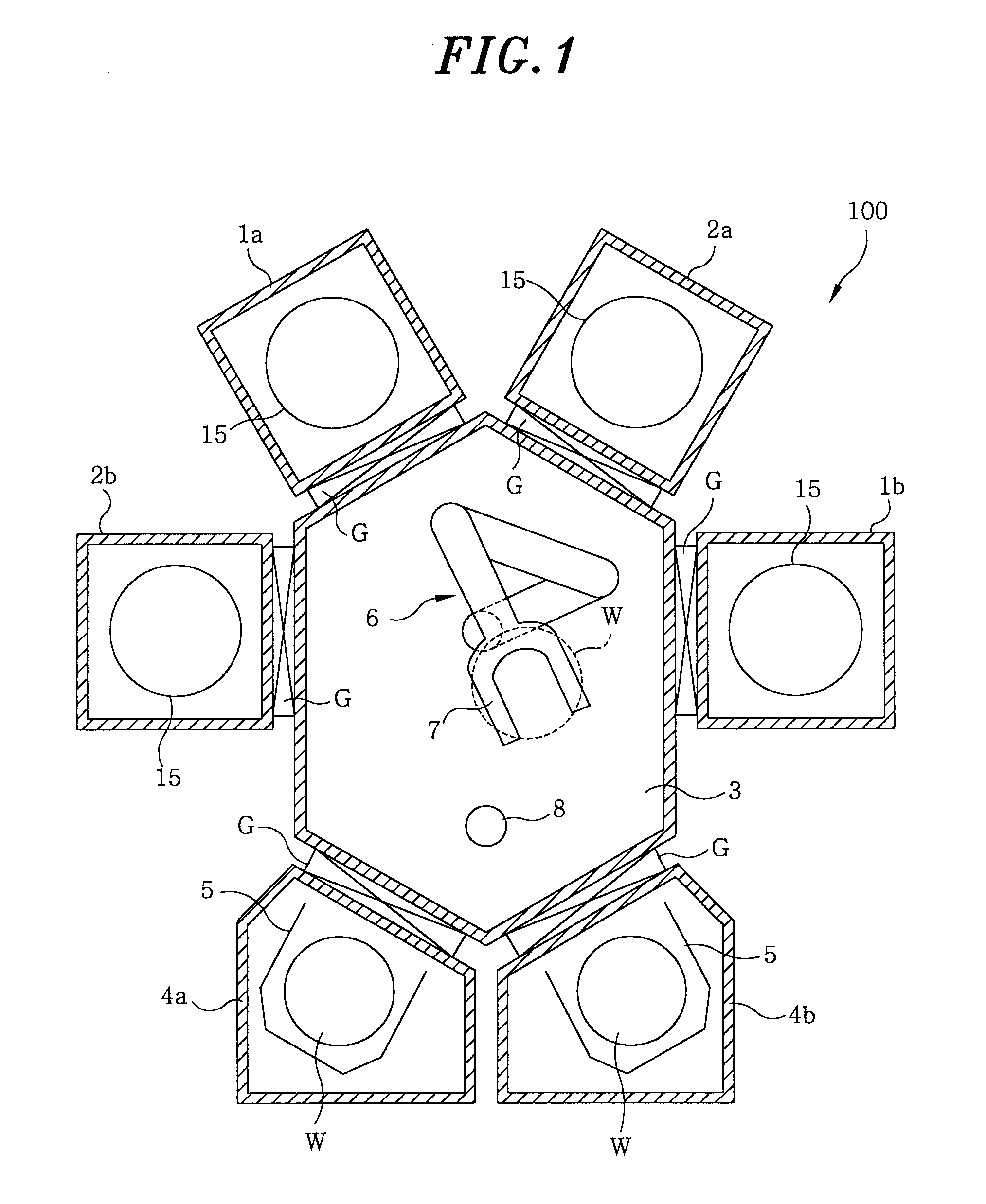
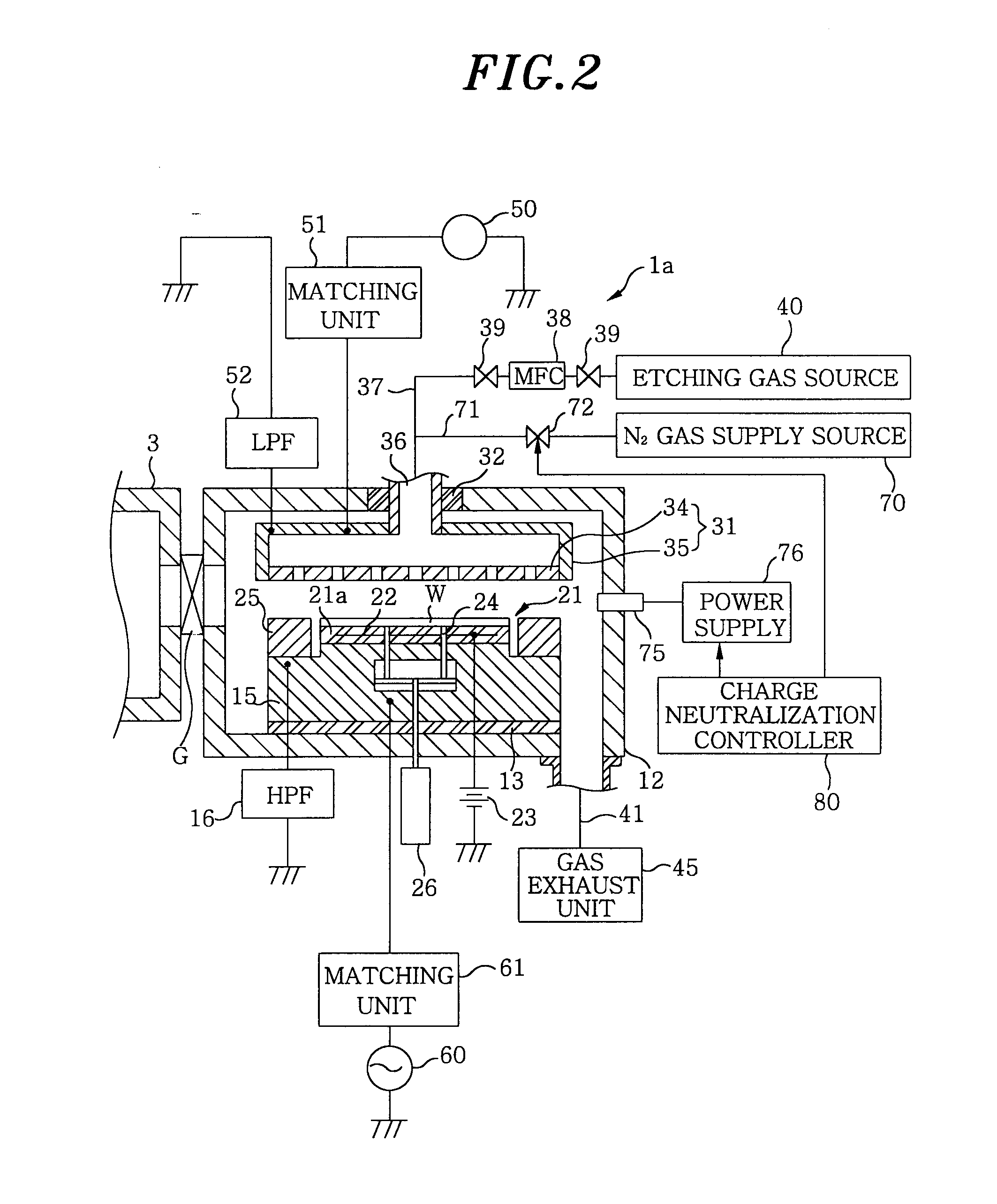
[0029]There is schematically illustrated in FIG. 1 a vacuum processing apparatus in accordance with a first embodiment of the present invention. The vacuum processing apparatus is a multichamber-type processing apparatus used in etching and ashing processes, for etching and ashing an object to be processed, such as a semiconductor wafer (hereinafter, referred to as “wafer”) under a predetermined level of vacuum.

[0030]As shown in FIG. 1, the multichamber-type processing apparatus 100 includes two etching chambers 1a, 1b for etching the wafer W, and two ashing chambers 2a, 2b for ashing the wafer W, wherein the etching and ashing chambers 1a, 1b, 2a, 2b are mounted on four sides of a hexagonal transfer chamber 3, respectively. The two remaining sides of the hexagonal transfer chamber 3 are provided with wafer cassette chambers 4a, 4b, respectively, whic...


PUM

PropertyMeasurementUnit
pressureaaaaaaaaaa
pressureaaaaaaaaaa
ionization energyaaaaaaaaaa

Abstract

A multichamber-type processing apparatus and processing method using same, in which a substrate is reliably neutralized without being damaged, thereby ensuring excellent accuracy and throughput. The processing apparatus includes a transfer chamber, etching chambers selectively communicating with the transfer chamber and providing a space to etch a first substrate therein, and ashing chambers selectively communicating with the transfer chamber and providing a space to ash a second substrate therein. A transfer mechanism is installed in the transfer chamber to sequentially transfer the substrate from the transfer chamber into the etching and ashing chambers. The substrate is electrostatically adsorbed to electrostatic chucks in the etching and ashing chambers. An monatomic nitrogen atom supply unit supplies dissociated monatomic nitrogen atoms into the etching and ashing chambers.

Description

CROSS-REFERENCE TO RELATED APPLICATIONS[0001]The present application is a division of application Ser. No. 10 / 814,258, filed on Apr. 1, 2004, which claims benefit of Japanese Patent Application No. 2003-098162 filed on Apr. 1, 2003. The entire contents of application Ser. No. 10 / 814,258 is incorporated hereinto by reference.FIELD OF THE INVENTION[0002]The present invention relates to a multichamber-type processing apparatus having an arrangement in which a transfer chamber is coupled to a plurality of processing chambers for etching or ashing a substrate to be processed, and a processing method using same.BACKGROUND OF THE INVENTION[0003]Generally, a multichamber-type processing apparatus, which includes a transfer chamber provided with a transfer arm and coupled to a plurality of processing chambers via gate valves, is known as a processing apparatus for performing etching, ashing, and deposition processes on a plurality of substrates, such as semiconductor wafers or glass substrat...

Claims


Application Information

Patent Timeline
Patent Type & Authority Applications(United States)
IPC IPC(8): B44C1/22B01J19/08H01L21/687H01L21/00H01L21/3065H01L21/306H01L21/68H01L21/683H01L21/768H05F3/06
CPCH01L21/67069H01L21/67167H01L21/76808H01L21/67236H01L21/6831H01L21/67207
Inventor ITO, TAKASHI
Owner TOKYO ELECTRON LTD
Why Eureka
Try Eureka