Wiring substrate and method of manufacturing same, and display device

a technology of wiring substrate and manufacturing method, applied in the direction of double resist layer, non-linear optics, instruments, etc., can solve the problems of inability to achieve sufficient pressure bonding, increase the tolerance range of alignment accuracy, and difficult mounting of driver ics

Inactive Publication Date: 2009-01-29
MITSUBISHI ELECTRIC CORP
View PDF2 Cites 9 Cited by
  • Summary
  • Abstract
  • Description
  • Claims
  • Application Information

AI Technical Summary

Benefits of technology

[0016]In accordance with one aspect, the present invention can provide a wiring substrate capable of increasing the tolerance range on the alignment accuracy in the mounting of an external circuit to mounting terminals and a method of manufacturing the same, and a display device.

Problems solved by technology

The distance between mounting terminals becomes so small in such narrow pitch that the mounting of a driver IC becomes very difficult.
As a result, the occurrence of continuity failure increases.
Furthermore, since the bump 12 does not fall into the opening 5, the conductive particles 14 located within the opening 5 are not properly squashed, and thereby sufficient pressure bonding cannot be achieved.
Therefore, even if the proper continuity is achieved immediately after the mounting, continuity failure may occur during use, and thereby it poses a problem in reliability.
As a result, electrical resistance between the bump 12 and the mounting terminal 6 increases, and continuity failure may occur.

Method used


Image

  • Wiring substrate and method of manufacturing same, and display device
  • Wiring substrate and method of manufacturing same, and display device
  • Wiring substrate and method of manufacturing same, and display device

Examples


first embodiment

[0034]Firstly, a display device in accordance with one example of the present invention is explained hereinafter with reference to FIG. 1. FIG. 1 is a front view showing the structure of a TFT array substrate for use in a display device. While a liquid crystal display device is explained as an example of the display device in the following embodiments, the explanation is made only for the illustrative purpose. For example, other flat-panel display devices, such as an organic electroluminescence display device can be used as a substitute for the liquid crystal display device. The overall structures of the liquid crystal display devices are substantially the same throughout the following first to fifth embodiments.

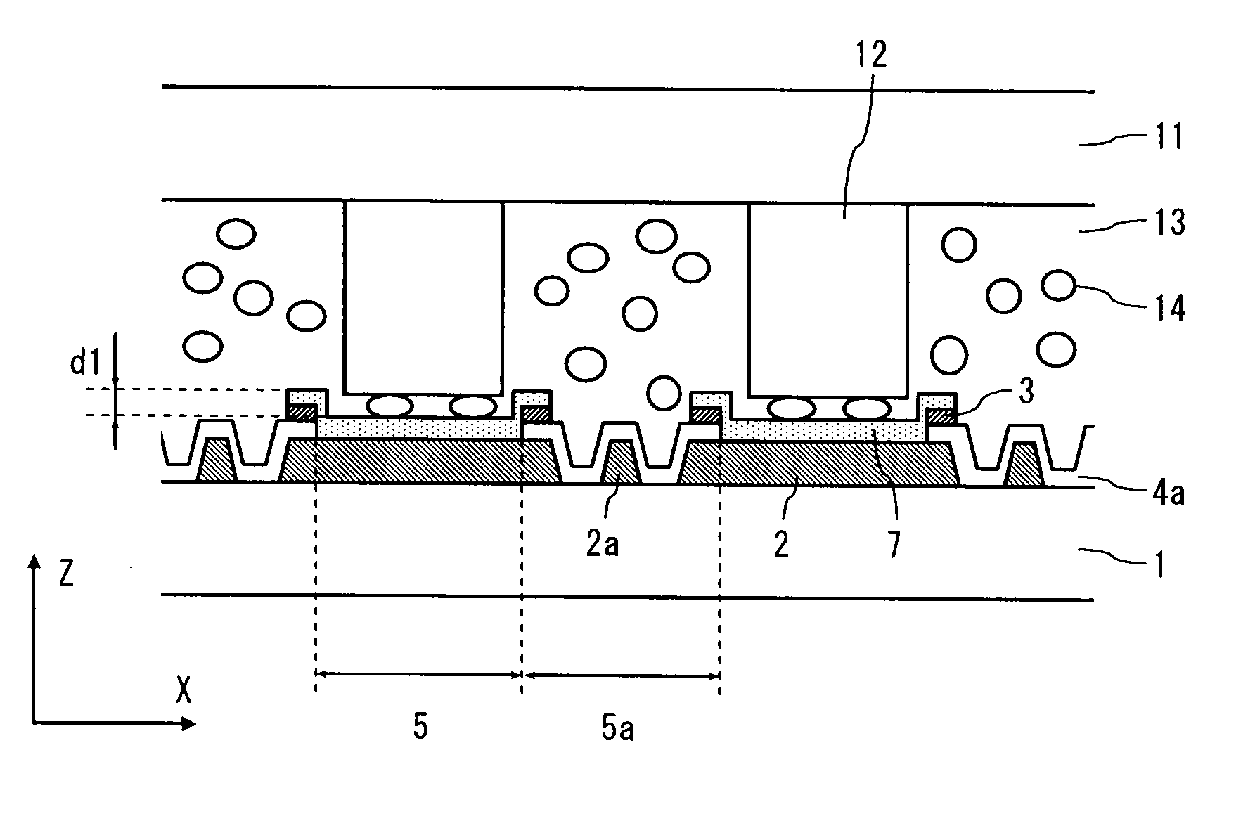
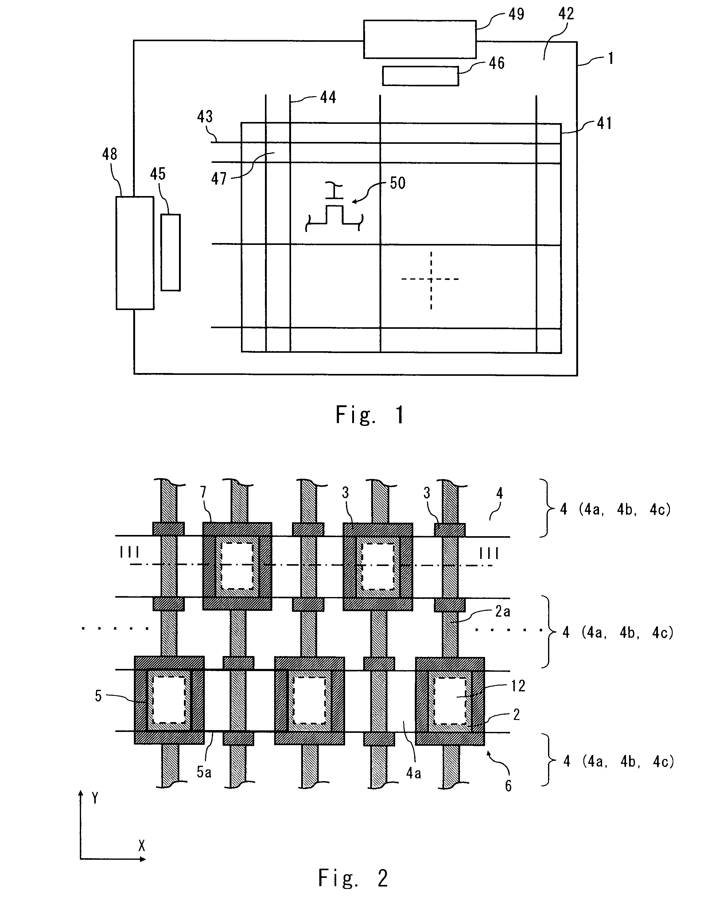
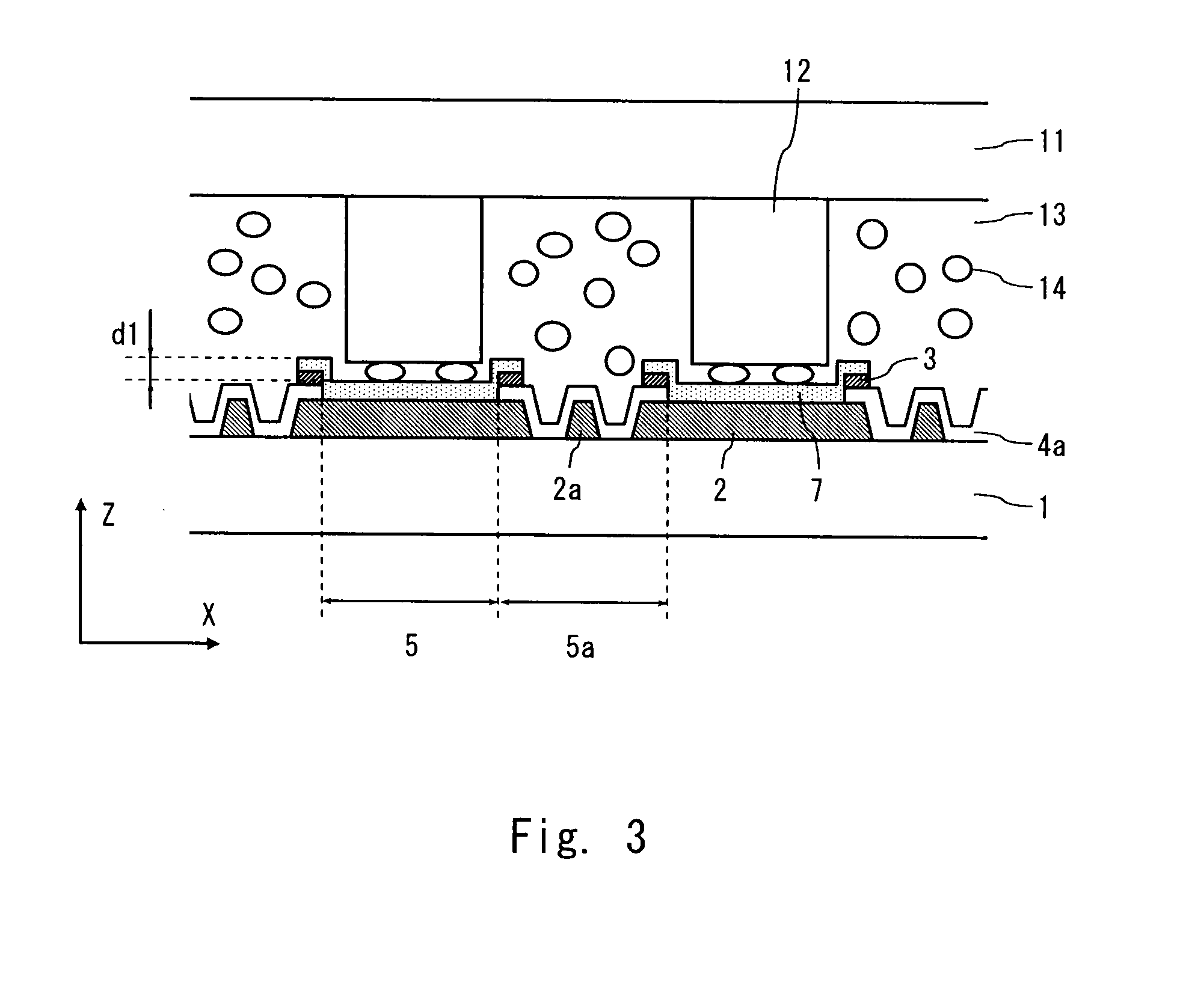
[0035]A liquid crystal display device in accordance with one example of the present invention has a substrate 1. The substrate 1 is, for example, an array substrate such as a TFT array substrate. A display area 41 and a frame area 42 surrounding the display area 41 are provi...

second embodiment

[0061]The structure of a mounting terminal in accordance with a second embodiment is explained in detail hereinafter with reference to FIGS. 5 and 6. FIG. 5 is a plane view showing the structure of mounting terminals of a liquid crystal display device in accordance with a second embodiment of the present invention. FIG. 6 is a cross-sectional view as taken along the line VI-VI in FIG. 5. This embodiment is different from the first embodiment in the structure of the mounting terminals. However, other structures are the same as the first embodiment, and therefore explanation of the other structures is omitted.

[0062]In FIGS. 5 and 6, the same signs are assigned to the potions having structures similar to those of FIGS. 2 and 3, and differences are explained. In FIG. 5, similarly to the first embodiment, mounting terminals 6 are arranged in several rows in a staggered pattern to accommodate a narrow pitch. In this embodiment, the staggered pattern of two rows is illustrated as an exampl...

third embodiment

[0074]The structure of a mounting terminal in accordance with a third embodiment is explained in detail hereinafter with reference to FIGS. 8 and 9. FIG. 8 is a plane view showing the structure of mounting terminals of a liquid crystal display device in accordance with a third embodiment of the present invention. FIG. 9 is a cross-sectional view as taken along the line IX-IX in FIG. 8. In this embodiment, the line 2a is further covered by a semiconductor layer in the thin film portion 5a. However, other structures are the same as the second embodiment, and therefore explanation of the other structures is omitted.

[0075]In FIGS. 8 and 9, the same signs are assigned to the potions having structures similar to those of FIGS. 5 and 6, and differences are explained. In FIGS. 8 and 9, similarly to the second embodiment, a line 2a is provided in the thin film portion 5a on the substrate 1, and an insulating film 4a is formed to cover the line 2a. In this embodiment, a semiconductor layer 8 ...


PUM


Abstract

A wiring substrate includes a plurality of lines provided on the substrate, and a plurality of mounting terminals each for respective one of the plurality of lines, the plurality of mounting terminals being arranged in several rows in a staggered pattern, wherein the mounting terminal includes a first conductive film formed in the same layer as the lines, an insulating film covering the lines and the first conductive film, the insulating film having an opening above the first conductive film, and an upper layer conducive film electrically connected to the first conductive film through the opening, and wherein the insulating film includes a thick film portion located on the outside of the area where the plurality of mounting terminals are arranged in several rows in the staggered pattern, and a thin film portion located in the area adjacent to the opening in the row direction of the staggered pattern with a thickness thinner than the thick film portion.

Description

BACKGROUND OF THE INVENTION[0001]1. Field of the Invention[0002]The present invention relates to a wiring substrate and a method of manufacturing the same, and a display device.[0003]2. Description of Related Art[0004]A liquid crystal display device is thin and light, and has low power consumption, and thereby has been used as a display device for various equipments. In particular, as mobile information equipment such as a mobile phone has become smaller and thinner, COG (Chip On Glass) mounting technique has been used more widely as a mounting method of a driver IC that is used to drive a liquid crystal display device in such equipment.[0005]In the COG mounting method, a driver IC is directly mounted on a glass substrate having mounting terminals formed on the substrate. In most cases, the driver IC is electrically connected to the mounting terminals through an ACF (Anisotropic Conductive Film) in the COG mounting (for example, see Japanese unexamined patent application publication...

Claims


Application Information

Patent Timeline
Patent Type & Authority Applications(United States)
IPC IPC(8): H01L29/04H01L21/84
CPCH05K1/112H05K3/323H05K3/3452H05K2201/0191H05K2203/0588H05K2201/09509H05K2201/09709H05K2203/0577H05K2201/09436G02F1/1345G02F1/133
Inventor HASHIGUCHI, TAKAFUMI
Owner MITSUBISHI ELECTRIC CORP
Why Eureka
Try Eureka