Rf ID Tag Device

a technology of rfid tag and position detection, applied in the direction of reradiation, instruments, near-field systems using receivers, etc., can solve the problems of low transmission output (conversion efficiency), considerable loss of received power, and short communication range, so as to maximize the reception efficiency of an antenna

Active Publication Date: 2009-02-05
KITAYOSHI HITOSHI
View PDF27 Cites 49 Cited by
  • Summary
  • Abstract
  • Description
  • Claims
  • Application Information

AI Technical Summary

Benefits of technology

[0030]By employing these configurations, it is made possible to achieve considerable effects as below.
[0031]Disequilibrium feeding and equilibrium system modulation (a three-terminal circuit for antenna operation) are employed, and therefore it is possible to achieve the effect of maximizing the reception efficiency of an antenna.
[0032]Also, by employing a circuit based on a combination of a stub resonance-based, impedance transformation boosting scheme and a ladder boosting scheme, it is possible to obtain a reception voltage of five times or more that of conventional schemes.
[0033]Further, by employing a QPSK modulation circuit, but based on passive modulation, it is made possible to transmit information in an amount twice that of the conventional method per unit of transmitting power.

Problems solved by technology

According to this, the conventional passive RFID tag device is basically configured as shown in FIG. 1, and therefore has a problem that its possible communication range is short for the following reasons.
(1) A response signal is created by frequently changing impedance Zv between antenna feeding points (1) and (2) to repeat reflection and absorption of incident radio waves, so that the transmission output (conversion efficiency) is low, and the load impedance Zv is applied between the feeding points (1) and (2), resulting in considerable loss of received power.

Method used


Image

  • Rf ID Tag Device
  • Rf ID Tag Device
  • Rf ID Tag Device

Examples


example 1

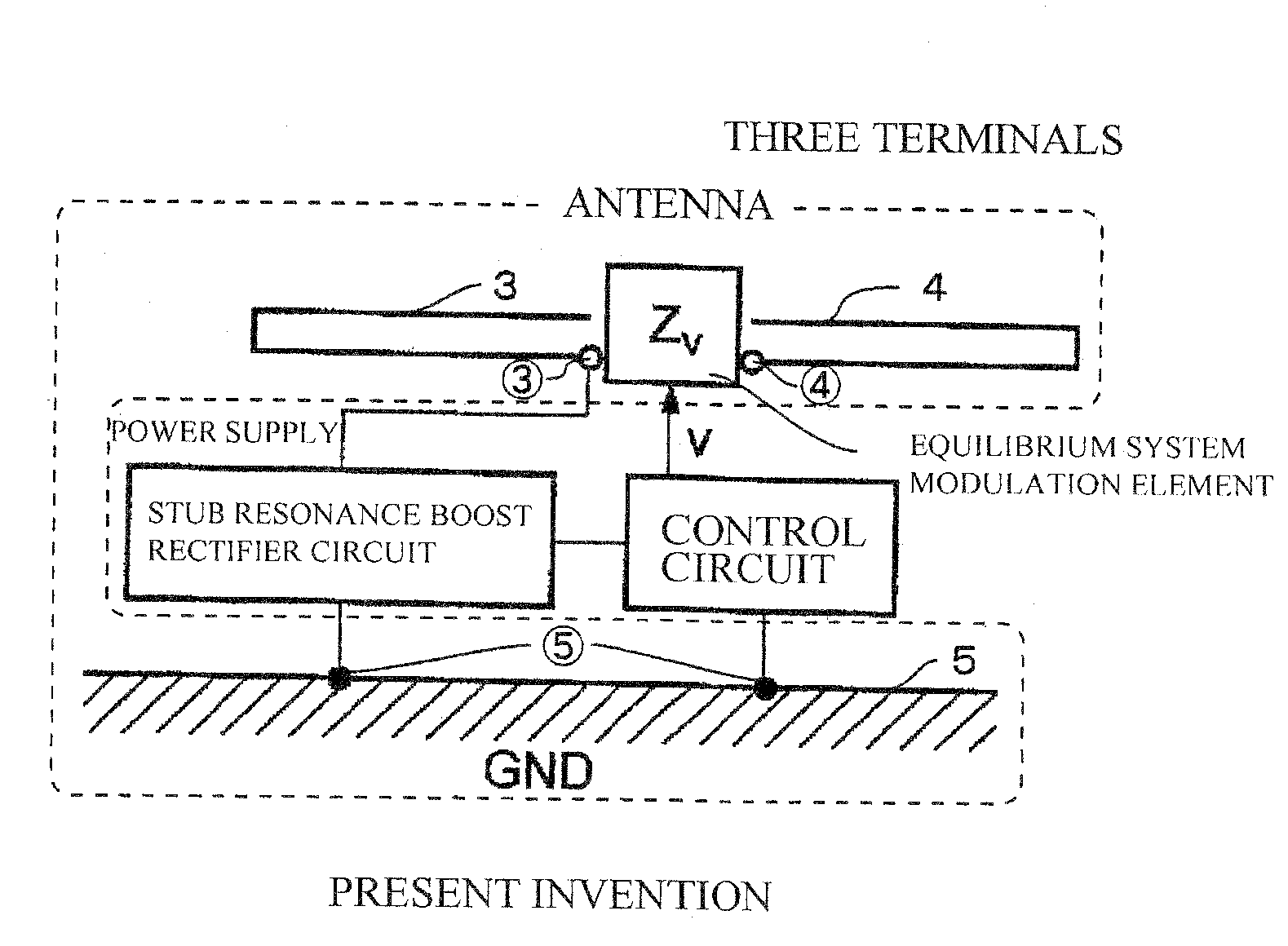
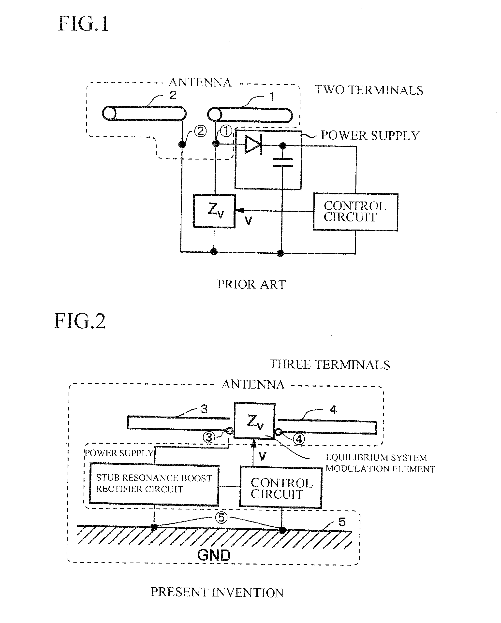
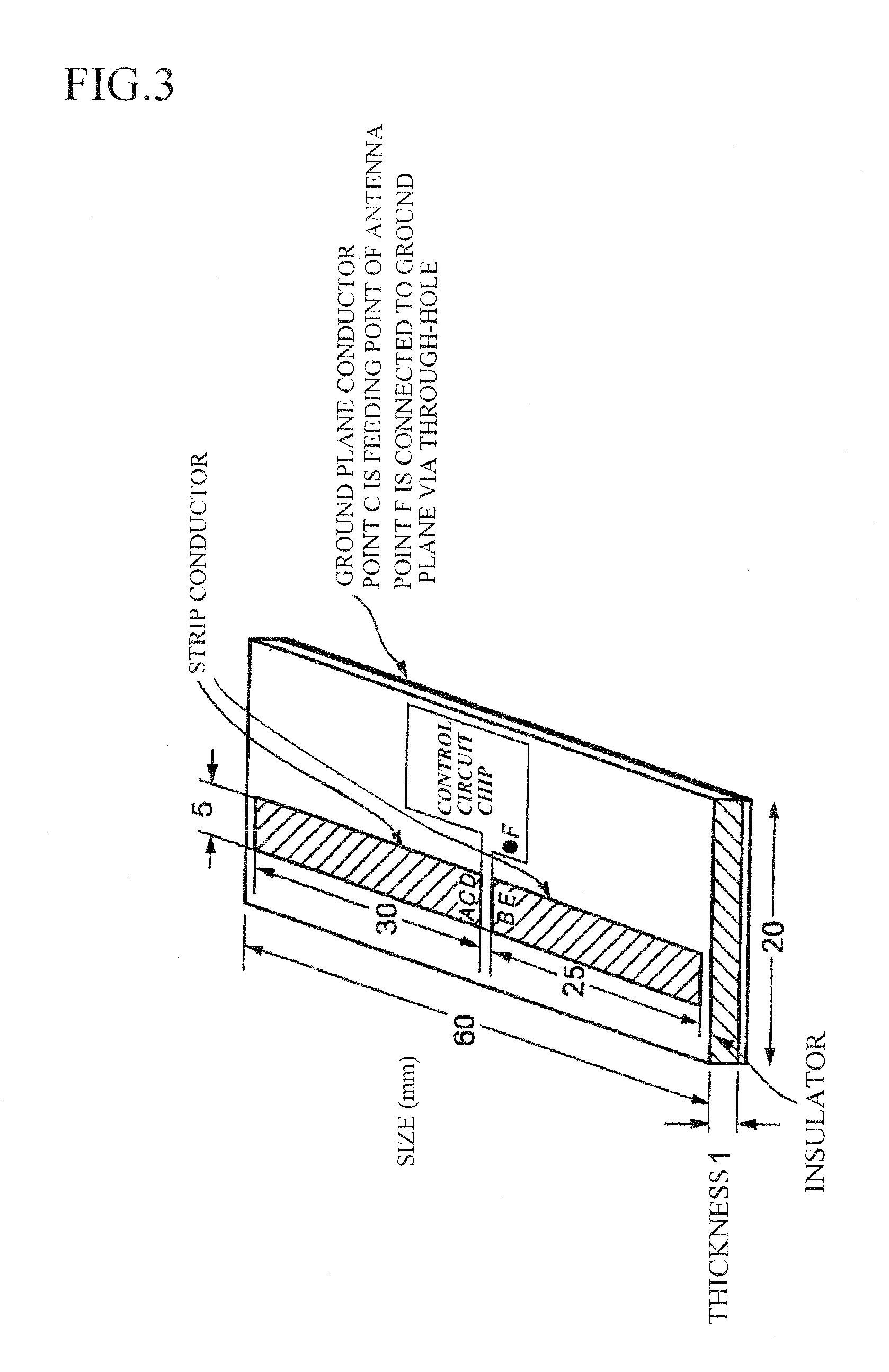
[0095]FIG. 3 illustrates the basic configuration of an RFID tag device of the present invention. In this figure, the antenna of the RFID tag device includes a ground plane conductor, an insulating layer and a divided strip conductor. The RFID tag device shown in this figure is for use in the 2.45 GHz band, and all specified dimensions are in units of mm. Also, the dividing point of the divided strip conductor is deviated slightly more than equal division in the longitudinal direction, and this feature achieves the effect of improving the reception efficiency of the antenna.

[0096]FIG. 4 illustrates the details of the control circuit chip shown in FIG. 3 and connections between the divided strip conductor and the control circuit.

[0097]In FIG. 4, the control circuit chip and the antenna are connected at six points A, B, C, D, E and F. PIN diodes D7 and D8 for impedance modulation are connected between A and B and between D and E, respectively, and a feeding point of the antenna lies be...

example 2

[0113](A method for detecting the position of a moving object without an RFID tag)

[0114]The feature of the RFID tag of the present invention that is capable of relatively long range communication in spite of having no power supply is utilized.

[0115]Assuming that the positions of tags #1 through #4 and interrogators #1 and #2 are known as shown in FIG. 6, it is possible to estimate the position of a mobile object based on information concerning paths obstructed by the moving object.

[0116]In this case, a system may be configured such that fm1=fm2, fs1=fs2=fs3=fs4, the interrogators provide CW outputs in a time-division system, and the tags respond by an anticollision method.

[0117]Further, a system may be configured such that fm1≢fm2, fs1=fs2=fs3=fs4, the interrogators successively provide CW outputs, and the tags respond by an anticollision method.

[0118]Furthermore, a system may be configured such that fm1≢fm2, fs1, fs2, fs3 and fs4 are all different frequencies, and the interrogators...

example 3

[0119](A method for detecting the position of a moving object with RFID)

[0120]The feature of the RFID tag of the present invention that is capable of relatively long range communication in spite of having no power supply is utilized.

[0121]As shown in FIGS. 22 and 23, a plurality of receiving antennas are used at the master device, and CW signals are transmitted at two or more frequencies to detect differences in phase between response signals from RFID tags, making it possible to estimate three-dimensional locations of the RFID tags.

[0122]FIG. 7 illustrates the configuration of a master device. A Fourier transform section performs time-series Fourier integration on Re and Im data of antennas #1 through #4 to calculate a spectrum phase at a frequency Δ. In this case, it is assumed that phase differences due to each antenna cable and down converter and a time delay in operations of a selecting switch are calibrated for the compensation.

[0123]Note that FIGS. 29 to 31 present an example...


PUM


Abstract

The present invention aims to overcome the drawback with conventional RFID tag devices having a short communication range, and expand the communication range to several times or more that in the conventional scheme. The conventional scheme is based on equilibrium feeding / equilibrium modulation (a two-terminal circuit for antenna operation), whereas the present invention is based on disequilibrium feeding / equilibrium modulation (a three-terminal circuit for antenna operation). The conventional scheme is based on simple rectification of received RF signals, whereas the present invention employs a circuit based on a combination of a stub resonance-based, impedance transformation boosting scheme and a ladder boosting scheme. The conventional scheme is based on ASK or BPSK modulation, whereas the present invention is based on passive modulation, but can employ a QPSK modulation circuit.

Description

TECHNICAL FIELD[0001]The present invention relates to RFID tag devices and position detection and communication methods using the same, and specifically to an RFID tag device based on passive modulation, but capable of performing, for example, QPSK modulation for wireless communication by using a loop antenna or a dipole antenna, and position detection and communication methods using the same.BACKGROUND ART[0002]Patent Document 1: Japanese Laid-Open Patent Publication No. 10-224262[0003](Tags for radio frequency identification communication systems)[0004]RFID is wireless equipment for identifying mobile objects, which is attached to or held by a commodity, a person, a car, a road sign, etc., and in response to a radio wave from an interrogator (a reader / writer), notifies individual information and position information to the interrogator.[0005]The RFID is considered not only as an alternative to the barcode, but also as elemental technology for implementing an entirely new infrastru...

Claims


Application Information

Patent Timeline
Patent Type & Authority Applications(United States)
IPC IPC(8): H04B1/59H01Q13/08H01Q9/16H04B5/02H02J17/00G06K19/07G06K19/077H01Q1/22H01Q1/24H01Q1/38H01Q9/06H01Q23/00
CPCG06K19/0723G06K19/07749H01Q1/2208H01Q1/248H01Q1/38H01Q9/065G01S13/79H01Q23/00H02J17/00H04B1/59G06K19/07786G01S7/023G01S13/765H01Q9/16H02J50/20H02J50/005H02J50/90H02J50/27H02J50/40H02J50/60
Inventor KITAYOSHI, HITOSHISAWAYA, KUNIO
Owner KITAYOSHI HITOSHI
Why Eureka
Try Eureka