

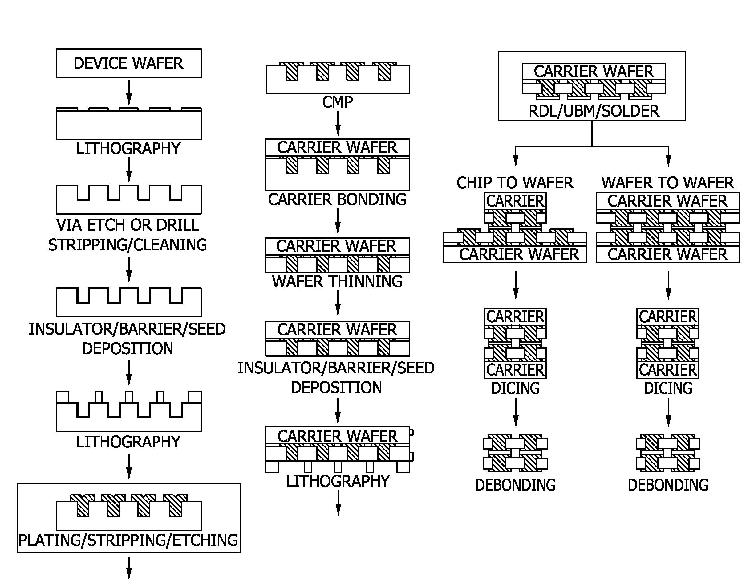
Copper metallization of through silicon via
a technology of copper metallization and through silicon, which is applied in the direction of basic electric elements, electrical apparatus, semiconductor devices, etc., can solve the problems of not revealing the duration necessary to achieve copper filling, and suggesting methods and compositions capable of rapid filling through silicon,
- Summary
- Abstract
- Description
- Claims
- Application Information
AI Technical Summary
Benefits of technology
Problems solved by technology
Method used
Image

Examples
example 1
Electrolytic Copper Deposition Using an Electrolytic Copper Deposition Composition of the Present Invention
[0086]An electrolytic copper deposition composition according to the present invention was prepared comprising the following components:
[0087]Cu(CH3SO3)2 (copper methane sulfonate sufficient to yield 100 g / L copper ions)
[0088]CH3SO3H (methane sulfonic acid, 10 g / L)
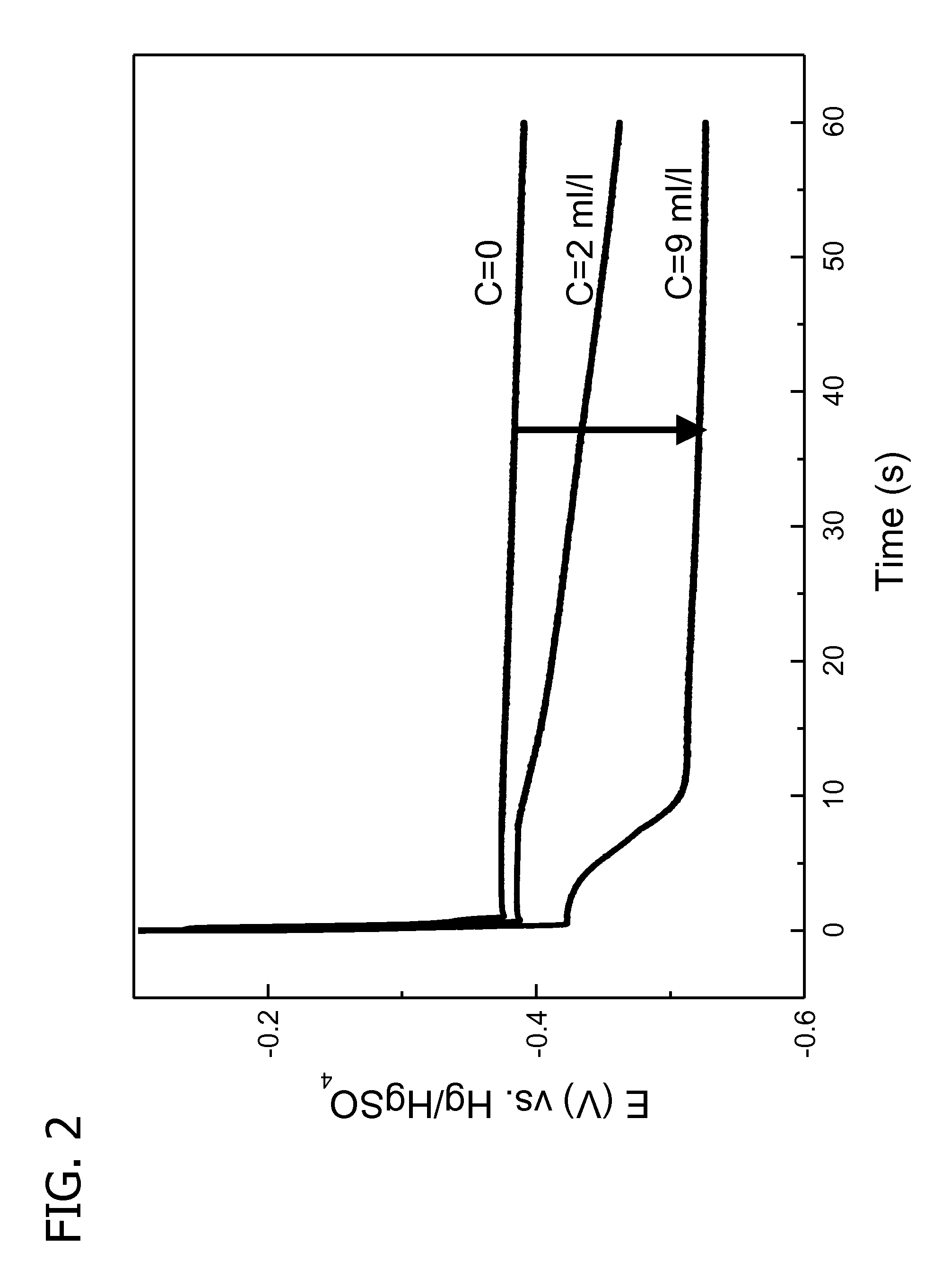
[0090]MICROVAB DVF 200 Additive C (available from Enthone Inc., West Haven, Conn.) (4 mL / L) containing methyl quaternized poly(vinyl-4-pyridine).
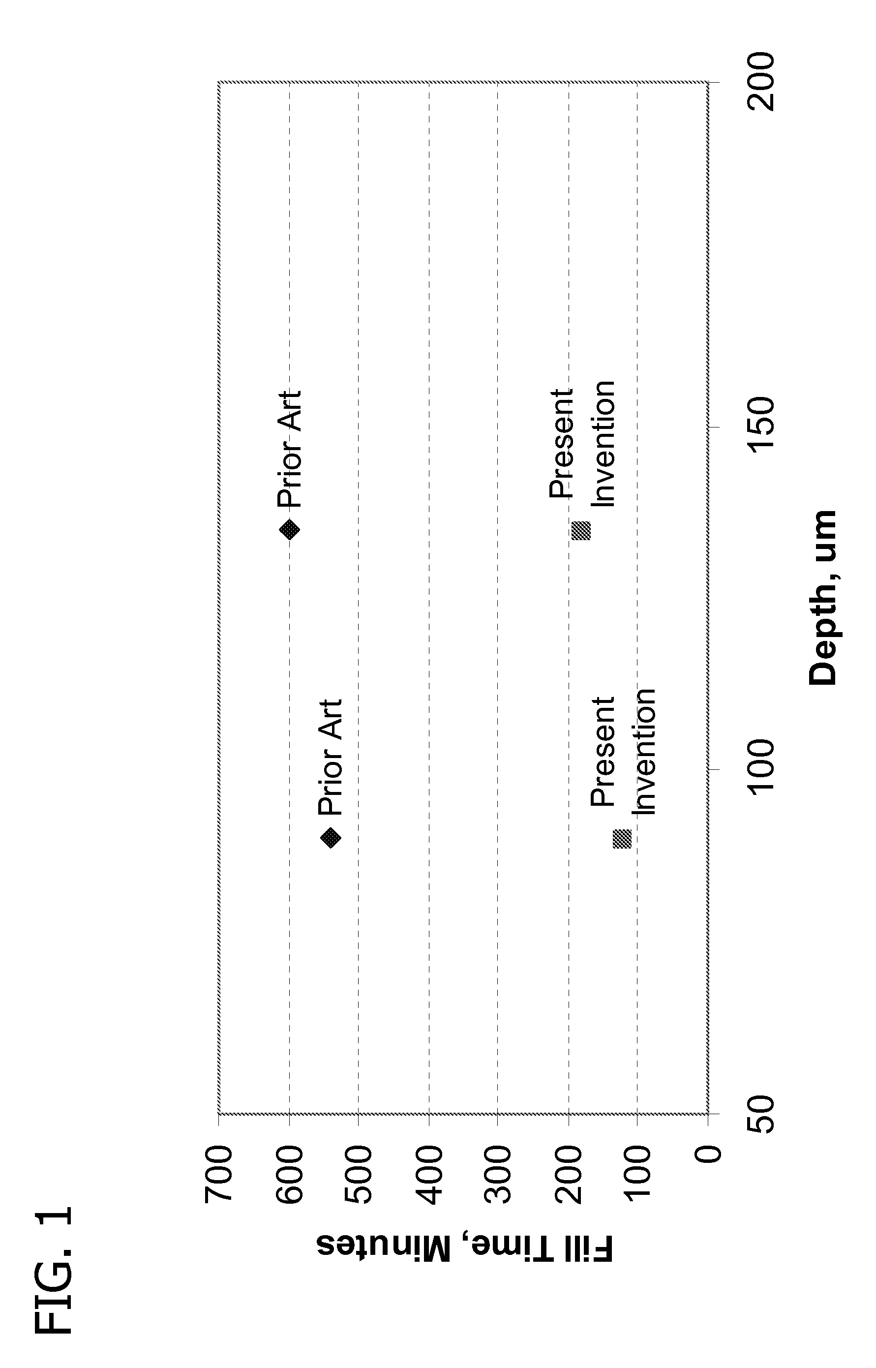
[0091]The vias had an aspect ratio of 2.5:1 (depth:opening diameter), resulting from an opening having a diameter of 100 microns and a total depth of 250 microns. In this example, the current density profile was characterized by relatively rapid increases to a maximum current density of 0.60 A / dm2.
[0092]The test wafer was degassed using MICROFAB® PW 1000 (available from Enthone Inc., West Haven, Conn.) and then immersed in the electrolytic copper de...
example 2
Electrolytic Copper Deposition Using an Electrolytic Copper Deposition Composition of the Present Invention
[0097]An electrolytic copper deposition composition according to the present invention was prepared comprising the following components:
[0098]Cu(CH3SO3)2 (copper methane sulfonate sufficient to yield 100 g / L copper ions)
[0099]CH3SO3H (methane sulfonic acid, 10 g / L)
[0101]MICROVAB DVF 200 Additives B & C (available from Enthone Inc., West Haven, Conn.):
[0102]MICROFAB DVF 200 B (4 mL / L)(containing 3,3′-dithiobis(1-propanesulfonic acid)
[0103]MICROFAB DVF 200 C (4 mL / L)
[0104]The vias had an aspect ratio of 1.75:1; 2.16:1; 3:1; and 5:1 (depth:opening diameter), resulting from an opening having the following diameters, respectively: 40, 30, 20, 10 microns, and the following depths, respectively: 70, 65, 60, 50 microns. In this example, the current density profile was characterized by relatively rapid increases to a maximum current density of 1.4 A / dm2.
[0105]...
example 3
Electrolytic Copper Deposition Using an Electrolytic Copper Deposition Composition of the Present Invention
[0112]An electrolytic copper deposition composition according to the present invention was prepared comprising the following components:
[0113]Cu(CH3SO3)2 (copper methane sulfonate sufficient to yield 100 g / L copper ions)
[0114]CH3SO3H (methane sulfonic acid, 10 g / L)
[0116]MICROVAB DVF 200 Additives B & C(available from Enthone Inc., West Haven, Conn.):
[0117]MICROFAB DVF 200 B (5.5 mL / L)
[0118]MICROFAB DVF 200 C (7 ml / L)
[0119]Polypropylene glycol amine (ca. 400 g / mol) 30 mg / L
[0120]The vias had an aspect ratio of 3.5:1; 3.8:1; 2.5:1; and 5:1 (depth:opening diameter), resulting from an opening having the following diameters respectively: 50; 45; 75; 35 microns; and all having a depth of 175 microns. In this example, the current density profile was characterized by relatively rapid increases to a maximum current density of 1.2 A / dm2.
[0121]The test wafer was ...
PUM
| Property | Measurement | Unit |
|---|---|---|
| depth | aaaaa | aaaaa |
| depth | aaaaa | aaaaa |
| depth | aaaaa | aaaaa |
Abstract
Description
Claims
Application Information