Photomask defect correction device and photomask defect correction method

Inactive Publication Date: 2009-02-12
SII NANOTECHNOLOGY INC
View PDF3 Cites 10 Cited by
  • Summary
  • Abstract
  • Description
  • Claims
  • Application Information

AI Technical Summary

Benefits of technology

[0022]The present invention has been made in view of the above-mentioned circumstances, and has an object to provide a photomask defect correction device and a photomask defect correction method with which it is possible to correctly obtain an image in a periphery on a root side of a defect portion without receiving an influence of a double chip image to recognize the defect portion and the mask pattern with clearly distinguished state, and is possible to remove the defect portion with high accuracy by means of cutting and removing processing.

Problems solved by technology

If the cutting and removing processing is performed from the root side towards the tip side (opposite direction to arrow A2 direction), there is a fear of being not able to cut well due to large cutting resistance.
However, in the above-mentioned conventional method, the following problems are remained unsolved.
Accordingly, from both the tip of the probe tip and the foreign matter X interatomic forces are detected and forms double image which is convoluted with both the interatomic forces (hereinafter, referred to as double chip image), thereby being not possible to obtain a correct image.
Moreover, there is such a risk that the defect portion 32 is scooped again due to the foreign matter X attached before, and as shown in FIG. 14, there is a fear of being newly attached with another foreign matter X.
As described above, there was a case of being not possible to obtain a normal image due to the influence of the foreign matter attached to the probe tip 33.
In particular, there is not much influence for the first observation, but in the case of performing the processing after the observation of multiple times, it is likely to cause a double chip image.
Specifically, the edge portion is blurred to be unclear or double, thereby being not able to obtain clear image.
In particular, it is not possible to correctly recognize the edge shape of the mask pattern 31, thereby being difficult to distinguish between the mask pattern 31 and the defect portion 32.
On the contrary, because the mask pattern 31 and the defect portion 32 may not be clearly distinguished therebetween, if the defect portion 32 is largely left uncut, additional processing is required, resulting in degradation of the working efficiency.

Method used


Image

  • Photomask defect correction device and photomask defect correction method
  • Photomask defect correction device and photomask defect correction method
  • Photomask defect correction device and photomask defect correction method

Examples


Embodiment Construction

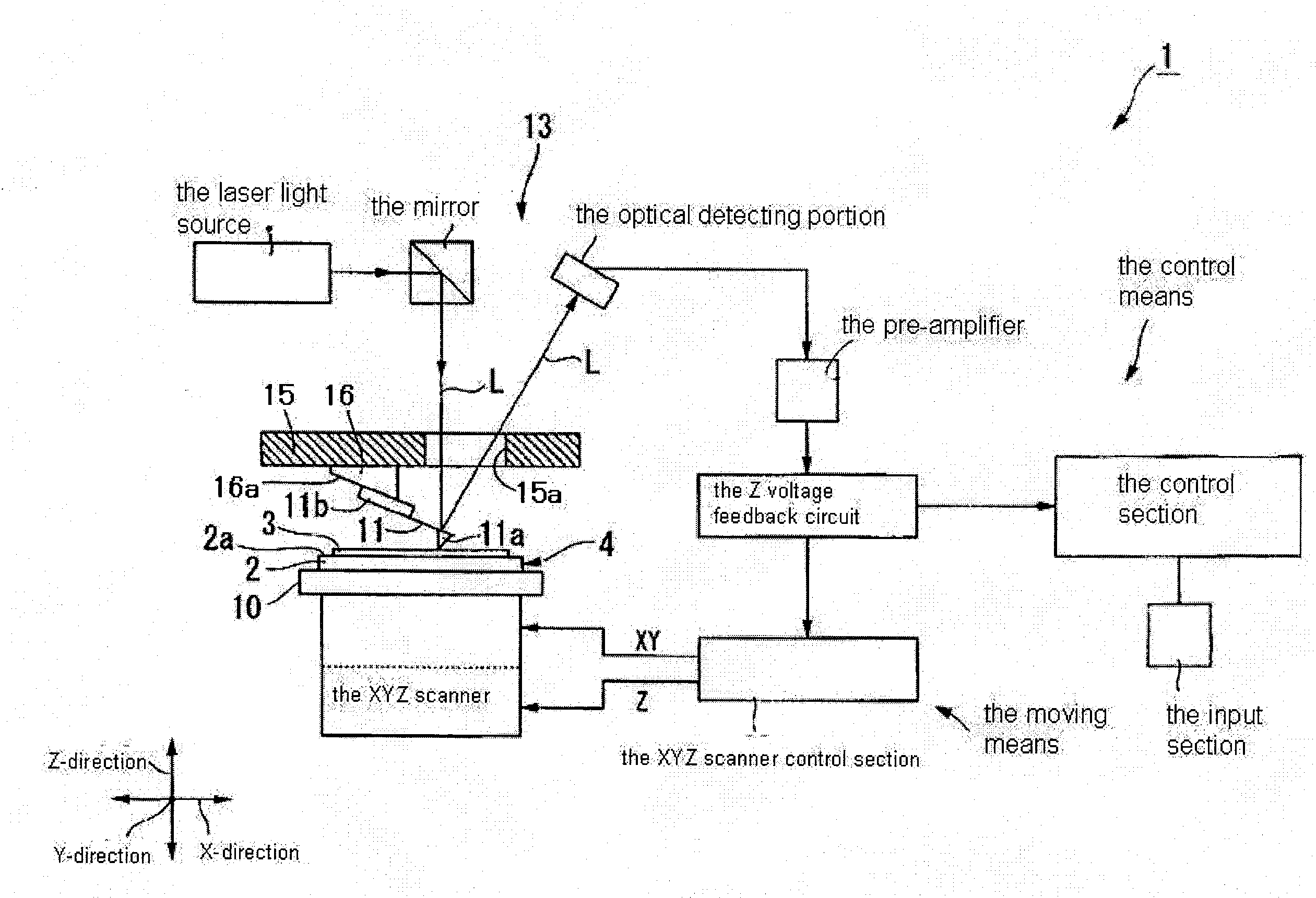
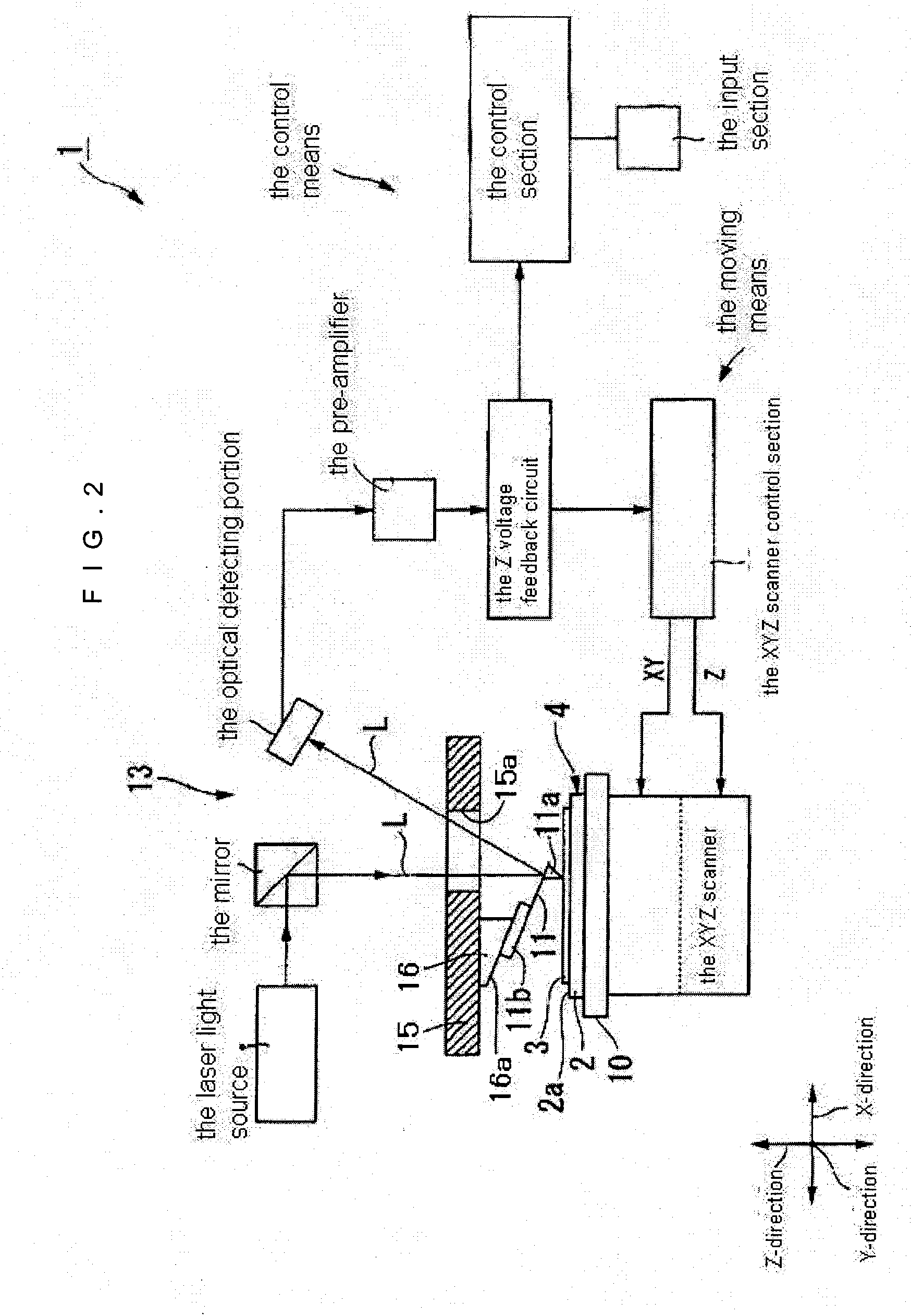
[0088]Hereinafter, description is made of an embodiment of a photomask defect correction device and a photomask defect correction method according to the present invention with reference to FIG. 1 to FIG. 8. Note that, in this embodiment, description is made of a case as an example where an optical lever method is used.

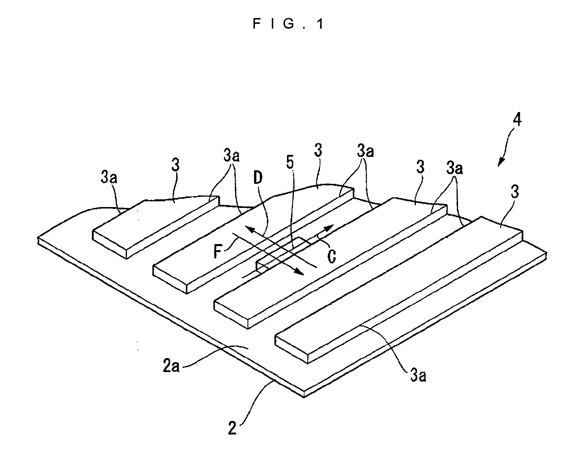
[0089]The photomask defect correction device 1 according to this embodiment performs AFM observation of a photomask 4 shown in FIG. 1, which includes a substrate 2 and a light-blocking film mask pattern (hereinafter, simply referred to as mask pattern) 3 formed on the substrate 2 so as to have a given pattern, a projection type of an excessive defect portion 5 (hereinafter, simply referred to as defect portion) projected from the mask pattern 3 is subjected to AFM observation to recognize a shape of the defect portion, and then the defect portion 5 is subjected to cutting and removing processing, to thereby correct the recognized defect portion 5.

[0090]Note that, the ...


PUM


Abstract

Provided is a photomask defect correction method including: an observing step of scanning plurality of lines one after another while controlling a distance between the probe tip and a surface (2a) of the substrate so that displacement of the probe becomes constant to recognize a shape of the defect portion (5) through AFM observation; and a processing step of scanning a plurality of lines one after another while pressing the probe tip to the recognized defect portion with a predetermined force to subject the defect portion to cutting and removing processing, in which, at the observing step, the scanning for every one line is set in a parallel direction (C direction) to an edge (3a) of a mask pattern (3), and the scanning of the plurality of lines is performed one after another from the mask pattern side towards a tip side (D direction) of the defect portion.

Description

RELATED APPLICATION[0001]This application claims priority under 35 U.S.C. §119 to Japanese Patent Application No. JP2007-165983 filed on Jun. 25, 2007, the entire content of which is hereby incorporated by reference.BACKGROUND OF THE INVENTION[0002]1. Field of Invention[0003]The present invention relates to a photomask defect correction device and a photomask defect correction method involving subjecting a defect portion of a photomask, which is used when manufacturing a semiconductor, to cutting and removing processing to correct the photomask into a normal one.[0004]2. Description of the Related Art[0005]The photomask, which is used when manufacturing a semiconductor, becomes an original plate for a pattern, and hence after drawing a mask pattern on a mask substrate, an inspection of presence or absence of the defect portion is always conducted, and the correction of the defect portion is optionally carried out.[0006]The photomask is drawn on the mask substrate with a drawing devi...

Claims


Application Information

Patent Timeline
IPC IPC(8): G01B5/28G01Q80/00G03F1/72G03F1/84H01L21/027
CPCB82Y10/00B82Y35/00G01Q10/06G03F1/84G01Q80/00G03F1/72G01Q30/06
Inventor NAKAUE, TAKUYAUEMOTO, ATSUSHITAKAOKA, OSAMU
Owner SII NANOTECHNOLOGY INC
Why Eureka
Try Eureka