Electron emission device for back light unit and liquid crystal display using the same

Inactive Publication Date: 2009-02-12
SAMSUNG SDI CO LTD
View PDF4 Cites 2 Cited by
  • Summary
  • Abstract
  • Description
  • Claims
  • Application Information

AI Technical Summary

Benefits of technology

[0011]An electron emission display device is provided that is capable of enhancing luminous efficiency by shortening a period that a signal is transmitted to a gate electrode, and of extending a life span of an emitter, by dividing a gate signal into a plurality of pulses and maintaining a predetermin

Problems solved by technology

If a high voltage is applied to a gate electrode, a cathode electrode, and an anode electrode, and a light emission time is made longer to represent bright grey levels, then the g

Method used


Image

  • Electron emission device for back light unit and liquid crystal display using the same
  • Electron emission device for back light unit and liquid crystal display using the same
  • Electron emission device for back light unit and liquid crystal display using the same

Examples


Embodiment Construction

[0031]Hereinafter, certain exemplary embodiments according to the present invention will be described with reference to the accompanying drawings. Herein, when a first element is described as being coupled to a second element, the first element may be not only directly coupled to the second element but may also be indirectly coupled to the second element via one or more third elements. Also, like reference numerals refer to like elements throughout.

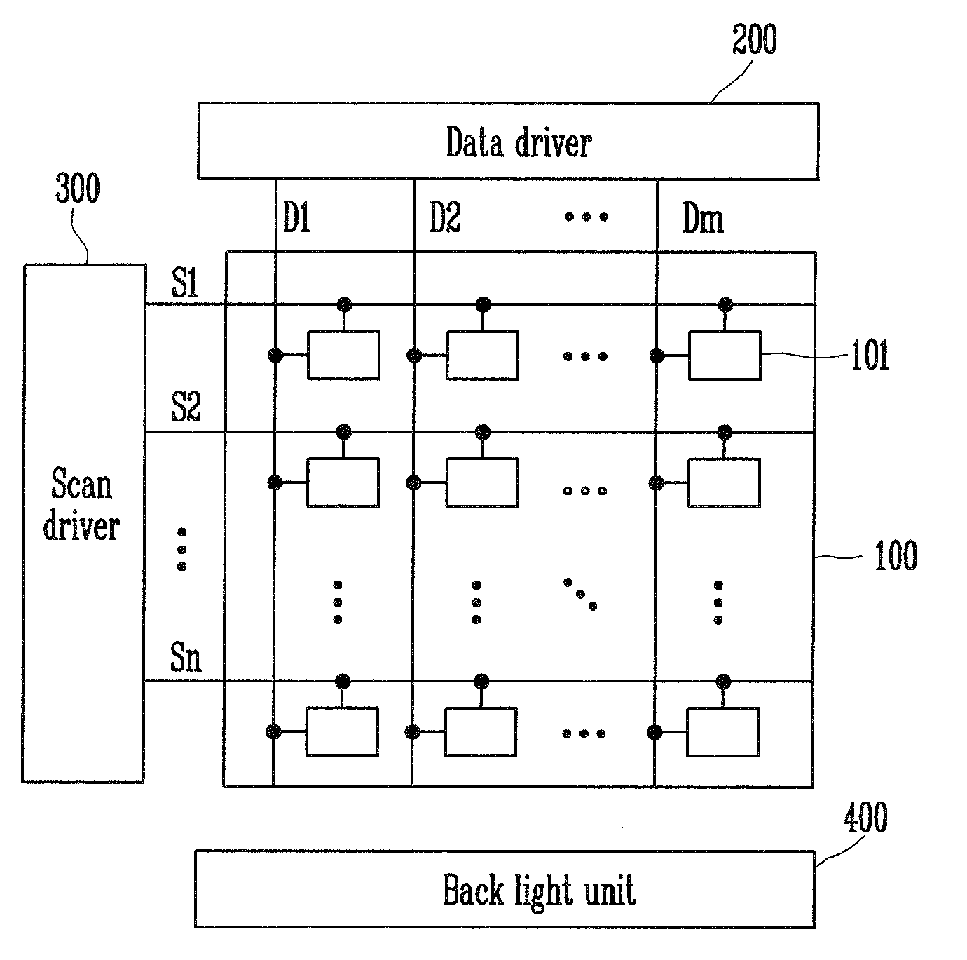
[0032]FIG. 2 is a configuration view showing a configuration of an electron emission display device according to an exemplary embodiment of the present invention. Referring to FIG. 2, the electron emission display device includes a light source unit 10, a cathode driver 20, and a gate driver 30.

[0033]The light source unit 10 has a plurality of light sources 11 formed in points where gate electrodes (G1, G2, . . . Gn) cross with cathode electrodes (C1, C2, . . . Cm), and electrons emitted from emitters coupled to the cathode electrodes (C1...


PUM


Abstract

An electron emission display device is provided having a light source unit including a plurality of cathode electrodes and a plurality of gate electrodes crossing the plurality of cathode electrodes. The light source unit emits electrons corresponding to voltages of the gate electrodes and the cathode electrodes and allows the emitted electrons to collide with a phosphor on an anode electrode to emit light. A gate driver generates a gate signal and transmits the gate signal to at least one of the gate electrodes. A cathode driver generates a cathode driving signal corresponding to an image signal and transmits the cathode driving signal to the cathode electrode. The cathode driving signal is transmitted in a plurality of pulse waveforms within one vertical synchronization period.

Description

CROSS-REFERENCE TO RELATED APPLICATION[0001]This application claims priority to and the benefit of Korean Patent Application No. 10-2007-0079524, filed on Aug. 8, 2007, in the Korean Intellectual Property Office, the entire content of which is incorporated herein by reference.BACKGROUND[0002]1. Field of the Invention[0003]The present invention relates to an electron emission device for a back light unit and a liquid crystal display, and more particularly to an electron emission device for a back light unit with enhanced luminous efficiency, and a liquid crystal display using the electron emission device.[0004]2. Description of the Related Art[0005]A flat panel display includes a plurality of pixels on a substrate in a matrix for use in a display area and includes scan lines and data lines coupled to the pixels for selectively applying a data signal to the pixels to display an image.[0006]A flat panel display can be categorized into a passive matrix type display device or an active m...

Claims


Application Information

Patent Timeline
IPC IPC(8): G09G3/20H01J1/62G02F1/1335G09G3/36
CPCG02F1/133602G02F2001/133625G09G3/22G09G3/3426G09G2320/0646G09G3/3648G09G2310/024G09G2320/0633G09G2320/064G09G3/3611G02F1/133625G02F1/133G09G3/36G09G3/20
Inventor LEE, JIN-SEOKLEE, JI-WONCHO, DUCK-GU
Owner SAMSUNG SDI CO LTD
Why Eureka
Try Eureka