

Heteroacene compound, organic thin film including a heteroacene compound and electronic device including an organic thin film
a heteroacene compound and organic thin film technology, applied in organic chemistry, luminescent compositions, chemistry apparatus and processes, etc., can solve the problems of low charge mobility and/or high off-state leakage current, and the use of low-molecular weight organic compounds requires costly equipment to form thin films using vacuum deposition, etc., to achieve the effect of increasing processability and high charge mobility
Inactive Publication Date: 2009-02-12
SAMSUNG ELECTRONICS CO LTD
View PDF1 Cites 39 Cited by
- Summary
- Abstract
- Description
- Claims
- Application Information
AI Technical Summary
Benefits of technology
This patent describes a new compound called a heteroacene, which has a compact structure with all six rings fused together. This compound has higher charge mobility and can be used in electronic devices. The patent also provides a method for making the compound and an organic thin film that can be used in electronic devices. The technical effect of this patent is to provide a new compound with improved properties for use in electronic devices.
Problems solved by technology
However, problems such as low charge mobility and / or high off-state leakage current may occur.
Although low-molecular-weight organic materials (e.g., pentacene) demonstrate a higher charge mobility of about 3.2 cm2 / Vs−5.0 cm2 / Vs or more, the use of low-molecular weight organic compounds requires costly equipment to form a thin film using vacuum deposition, which may be undesirable when preparing a film having a substantially large surface area.
Method used
View moreImage
Smart ImageViewing Examples

Examples
example 1
[0073]On a washed glass substrate, aluminum (Al) for a gate electrode was deposited to a thickness of 1000 Å by sputtering. An organic and inorganic hybrid insulating material (a mixture of silane compound and titanium butoxide) was applied through spin casting and dried at 200° C. for 2 hours, forming a gate insulating layer having a thickness of 7000 Å. Gold (Au) for source / drain electrodes was deposited thereon to a thickness of 700 Å through thermal evaporation. The compound synthesized in Preparative Example 1 was deposited to a thickness of 700 Å by thermal evaporation to form an organic semiconductor layer, fabricating an organic thin film transistor (OTFT).
Login to View More PUM
| Property | Measurement | Unit |
|---|---|---|
| temperature | aaaaa | aaaaa |
| temperature | aaaaa | aaaaa |
| structure | aaaaa | aaaaa |
Abstract
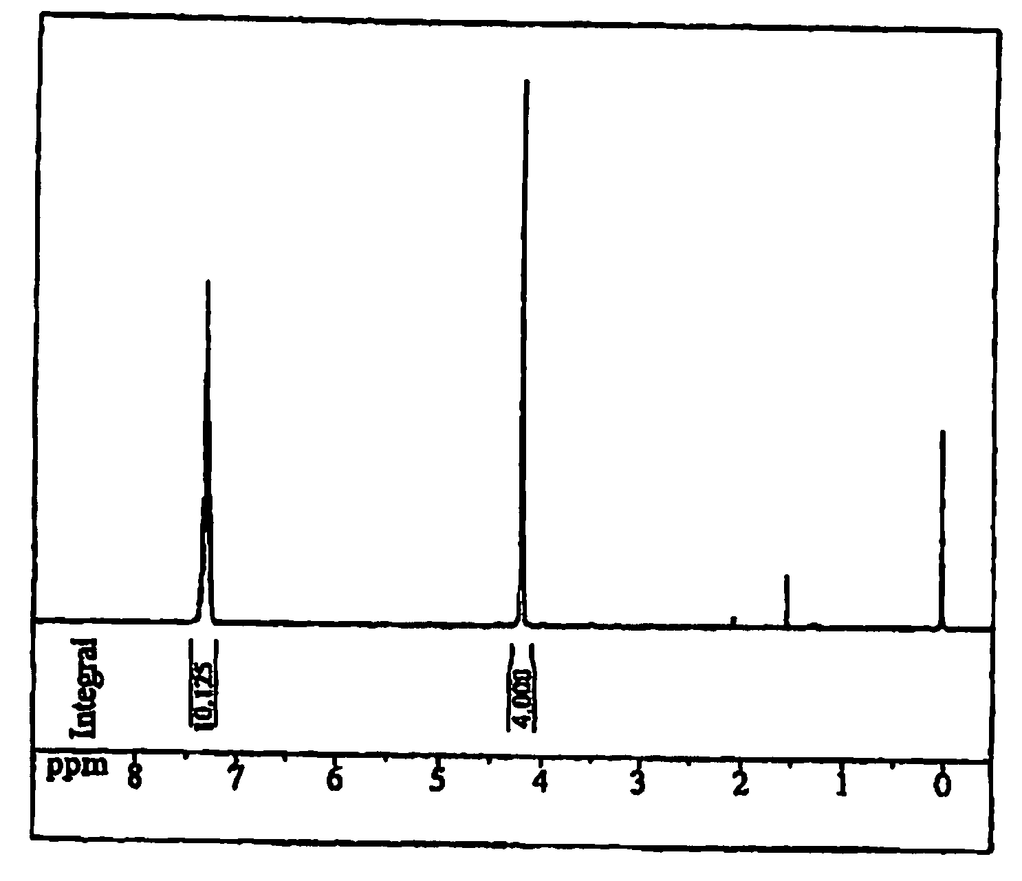
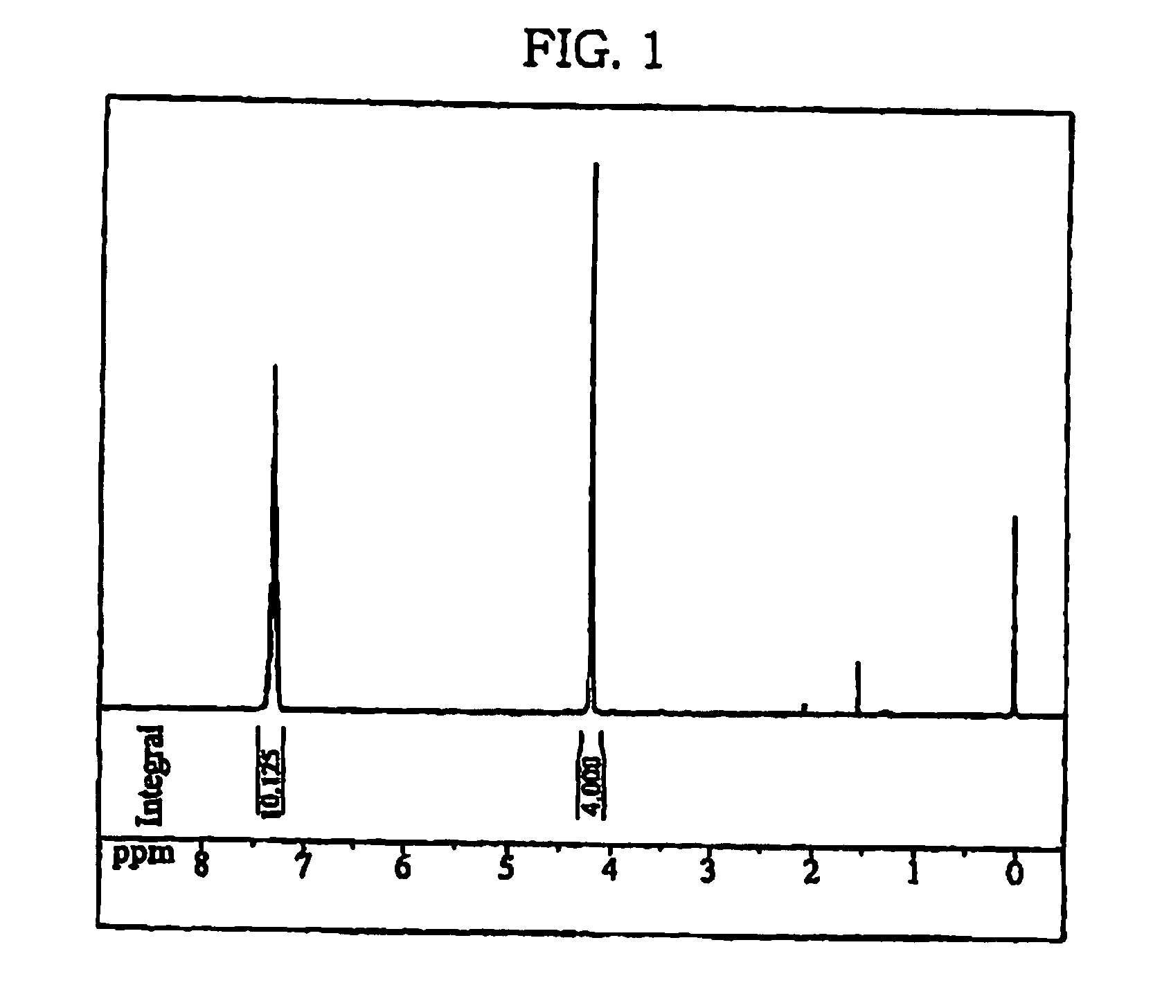
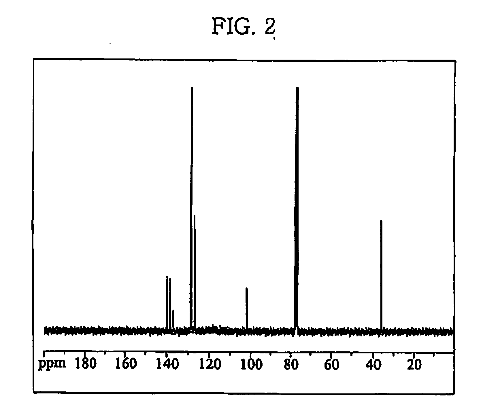
A heteroacene compound, an organic thin film including a heteroacene compound and an electronic device including a thin film are provided. The heteroacene compound is a compound having six rings fused together in a compact planar structure. The compound may be used in an organic thin film and / or applied to electronic devices using a deposition process or a room-temperature solution process.
Description
PRIORITY STATEMENT[0001]This non-provisional application claims the benefit of priority under U.S.C. § 119 from Korean Patent Application No. 10-2007-0047087, filed on May 15, 2007 with the Korean Intellectual Property Office (KIPO), the entire contents of which are herein incorporated by reference.BACKGROUND[0002]1. Field[0003]Example embodiments relate to a heteroacene compound, an organic thin film including the same and an electronic device including an organic thin film. Other example embodiments relate to a heteroacene compound, in which all six rings are fused together, an organic thin film including a heteroacene compound, and an electronic device that includes the thin film as a carrier transport layer.[0004]2. Description of the Related Art[0005]In general, flat display devices (e.g., liquid crystal displays, organic electroluminescent displays or the like) are provided with a variety of thin film transistors (TFTs) to drive them. A TFT may include a gate electrode, source...
Claims
Login to View More Application Information
Patent Timeline
 Patent Type & AuthorityApplications(United States)
IPC IPC(8): C07D333/50
CPCC07D495/04Y02E10/549H01L51/0545H01L51/0074H10K85/6576H10K10/466C09K11/06
InventorPARK, JEONG ILJEONG, EUN JEONGLEE, SANG YOON
OwnerSAMSUNG ELECTRONICS CO LTD