Heterojunction field effect transistor and manufacturing method thereof

a technology of junction field and transistor, which is applied in the direction of basic electric elements, electrical apparatus, and semiconductor devices, etc., can solve the problems of short channel effect, affecting the yield rate, and cracks on the surface of alsub>x/sub>gasub>

Inactive Publication Date: 2009-02-19
OKI ELECTRIC IND CO LTD
View PDF2 Cites 19 Cited by
  • Summary
  • Abstract
  • Description
  • Claims
  • Application Information

AI Technical Summary

Benefits of technology

[0027]The present invention is intended to solve the above described problems, and an object of the present invention is to provide ...

Problems solved by technology

However, the reduction of the gate length Lg may cause a “short channel effect” such as a degradation of pinch-off characteristics, a negative shift of threshold voltage or the like.
Further, the shift of threshold voltage narrows the tolerance with respect to the design value, and affects the yield rate or the like.
However, in the case where AlxGa1-xN is grown using MOCVD (Metal Organic Chemical Vapor Deposition) method, if the concentration of Al in the AlxGa1-xN is increased, cracks may occur on the surface of the AlxGa1-xN layer when x is approximately 0.52, and affect the FET...

Method used


Image

  • Heterojunction field effect transistor and manufacturing method thereof
  • Heterojunction field effect transistor and manufacturing method thereof
  • Heterojunction field effect transistor and manufacturing method thereof

Examples


first embodiment

[0045]The heterojunction field effect transistor of the first embodiment will be described with reference to FIG. 1. The heterojunction field effect transistor is a high electron mobility transistor (HEMT). Therefore, in the following description, the heterojunction field effect transistor is also referred to as HEMT.

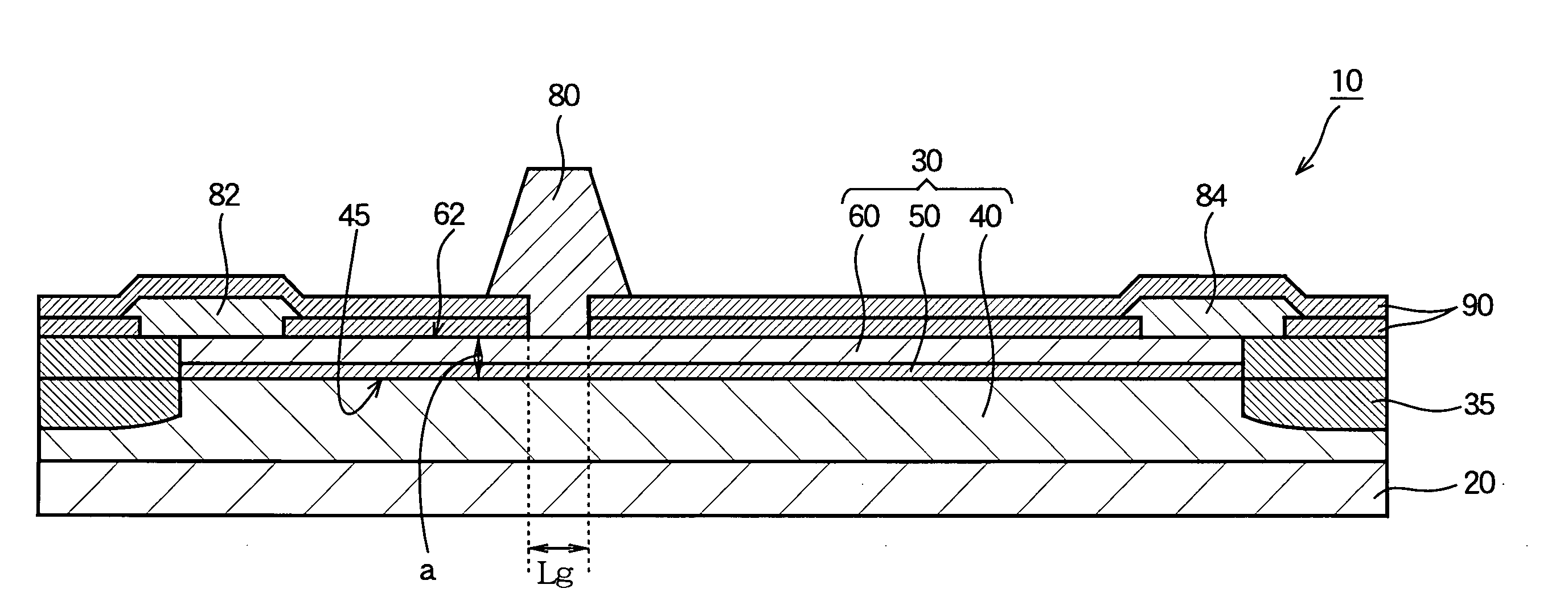
[0046]FIG. 1 is a sectional view schematically showing the heterojunction field effect transistor according to the first embodiment.

[0047]The heterojunction field effect transistor 10 according to the first embodiment includes a substrate 20 and a laminated body 30 formed on the substrate 20. The laminated body 30 includes a channel layer of GaN (i.e., a first GaN layer), an electron supply layer 50 of AlN (i.e., an AlN layer) and a cap layer 60 of GaN (i.e., a second GaN layer) laminated in this order on the substrate 20. Two dimensional electron gas (2DEG) is formed at an AlN / GaN heterointerface 45 between the channel layer 40 (the first GaN layer) and the electron su...

second embodiment

[0074]Next, a heterojunction field effect transistor according to the second embodiment of the present invention will be described with reference to FIG. 7. FIG. 7 is a sectional view schematically showing the heterojunction field effect transistor according to the second embodiment.

[0075]The heterojunction field effect transistor 11 according to the second embodiment has a MIS (Metal Insulator Semiconductor) structure in which a silicon nitride (SiN) film is formed as a gate insulation film 92 on the laminated body 30, and a gate electrode 80 is formed on the gate insulation film 92. A surface protection film 94 is formed on the gate insulation film 92. The field effect transistor having the MIS structure is called as MIS-FET. The structure of the laminated body 30 is the same as that of the first embodiment.

[0076]By employing the MIS structure, the gate leak current can be restricted. Even in the case where the silicon nitride film having the thickness of 14 nm is formed as the ga...

third embodiment

[0085]Next, a heterojunction field effect transistor according to the third embodiment will be described. FIG. 10 is a sectional view schematically showing the heterojunction field effect transistor according to the third embodiment.

[0086]The heterojunction field effect transistor 12 according to the third embodiment includes a laminated body 32 in which the channel layer 40 (the GaN layer) and the electron supply layer 50 (the AlN layer) are laminated in this order on the substrate 20. Two dimensional electron gas (2DEG) is formed in the AlN / GaN heterointerface 45 between the channel layer 40 and the electron supply layer 50.

[0087]In this third embodiment, a silicon nitride film as a gate insulation film 92 is formed on the electron supply layer 50 (the AlN layer). A surface protection film 94 is formed on the gate insulation film 92. The channel layer 40 (the GaN layer) and the electron supply layer 50 are formed using the MOCVD method as described in the second embodiment. The si...


PUM


Abstract

A heterojunction field effect transistor includes a laminated body. The laminated body includes a channel layer of GaN, an electron supply layer of AlN or AlxGa1-xN (0.6≦x<1) formed on the channel layer, and a cap layer of GaN formed on the electron supply layer.

Description

BACKGROUND OF THE INVENTION[0001]This invention relates to a heterojunction field effect transistor and a manufacturing method thereof, and particularly relates to a heterojunction field effect transistor having an electron supply layer of an AlN or AlxGa1-xN (0.6≦x<1) and a manufacturing method thereof.[0002]A conventional heterojunction field effect transistor will be described with reference to FIG. 11. FIG. 11 is a sectional view schematically showing a conventional heterojunction field effect transistor.[0003]The heterojunction field effect transistor 110 includes a substrate 120, a channel layer 140 of GaN formed on the substrate 120, and an electron supply layer 150 of AlGaN formed on the channel layer 140. The heterojunction field effect transistor 110 has a heterostructure of the channel layer 140 (GaN) and the electron supply layer 150 (AlGaN). With such a structure, it is possible to obtain high density two-dimensional electron gas (2DEG) and high electron mobility at ...

Claims


Application Information

Patent Timeline
IPC IPC(8): H01L29/778H01L21/31
CPCH01L21/0254H01L21/0262H01L21/3185H01L29/7787H01L29/42316H01L29/518H01L29/66462H01L29/2003H01L21/0217
Inventor HOSHI, SHINICHITAMAI, ISAOTODA, FUMIHIKO
Owner OKI ELECTRIC IND CO LTD
Why Eureka
Try Eureka