Wiring board for mounting semiconductor device, manufacturing method of the same, and wiring board assembly

Inactive Publication Date: 2009-02-19
RENESAS ELECTRONICS CORP +1
View PDF6 Cites 92 Cited by
  • Summary
  • Abstract
  • Description
  • Claims
  • Application Information

AI Technical Summary

Benefits of technology

[0073]The step for forming the two wiring boards can also includes a step for forming the conductive layer to be the electrode pad on a supporting base for at least one of the boards. A step for removing the supporting base entirely or partially can be included after the step for sticking. In this case, the supporting base can be a metal plate. The electrode pads are formed on the first and second supporting bases such as metal plates and the first and second dielectric films are formed on the electrode pads on the first and second supporting bases respectively. After that, the first and second dielectric films are stuck together, and then a dielectric film is formed by removing the first and second supporting plates. In this cases since the electrode pads are formed on the first and second supporting base with excellent flatness, exposed surfaces of the electrode pads are positioned accurately and densification is facilitated.
[0074]Additionally, since the two wiring boards formed on the supporting bases are stuck together face to face, the wiring board for mounting semiconductor device can be formed which is more accurate in alignment in the sticking, and more excellent in densification and reliability compared with a conventional simultaneously-stacked multilayer wiring board formed by simultaneously stacking a plurality of resin sheets. There is also an advantage that the number of layers can be increased in a short period of time compared with a conventional build-up board.
[0075]When stacking is performed at too high temperature and too high pressure in the sticking the two wiring boards formed on the supporting bases together face to face, there is a problem that reliability is deteriorated as a result of the occurrence of distortion of the wiring boards formed in advance on the supporting bases. In the case of the w

Problems solved by technology

This solves a problem that because a conventional wiring board has a structure in which wirings are provided to the front and back surfaces of a dielectric film positioned inside, stripping at the interface of the diel

Method used


Image

  • Wiring board for mounting semiconductor device, manufacturing method of the same, and wiring board assembly
  • Wiring board for mounting semiconductor device, manufacturing method of the same, and wiring board assembly
  • Wiring board for mounting semiconductor device, manufacturing method of the same, and wiring board assembly

Examples


Example

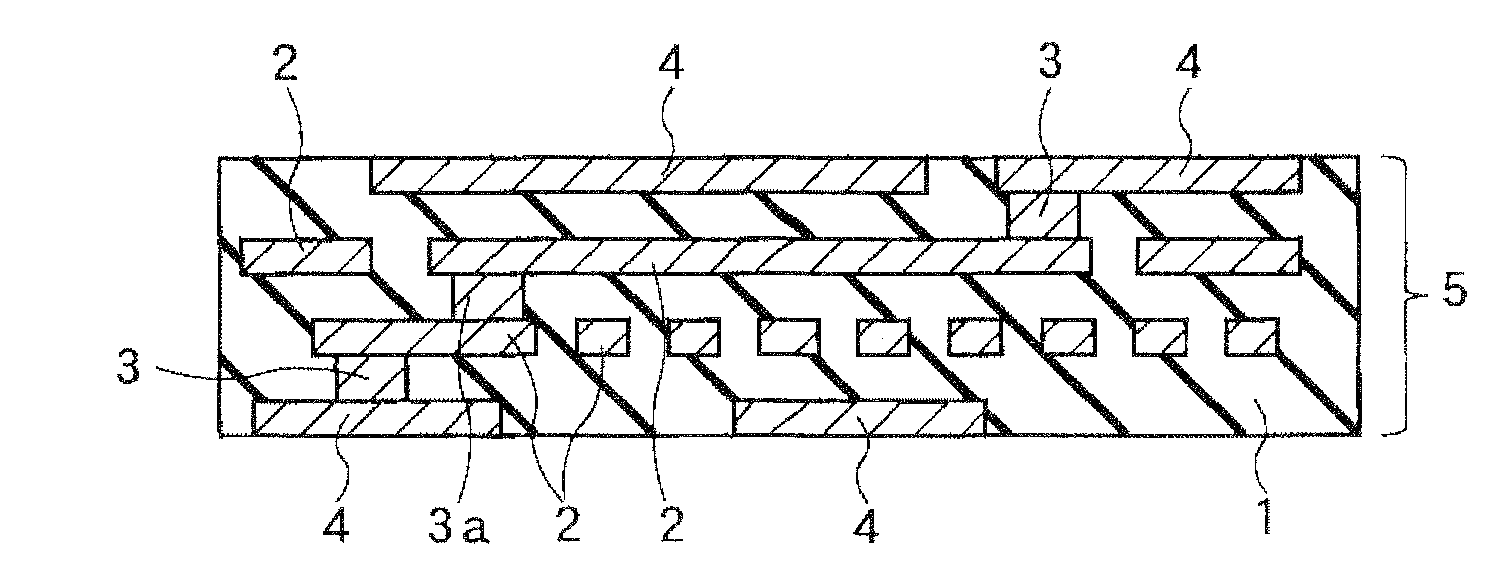
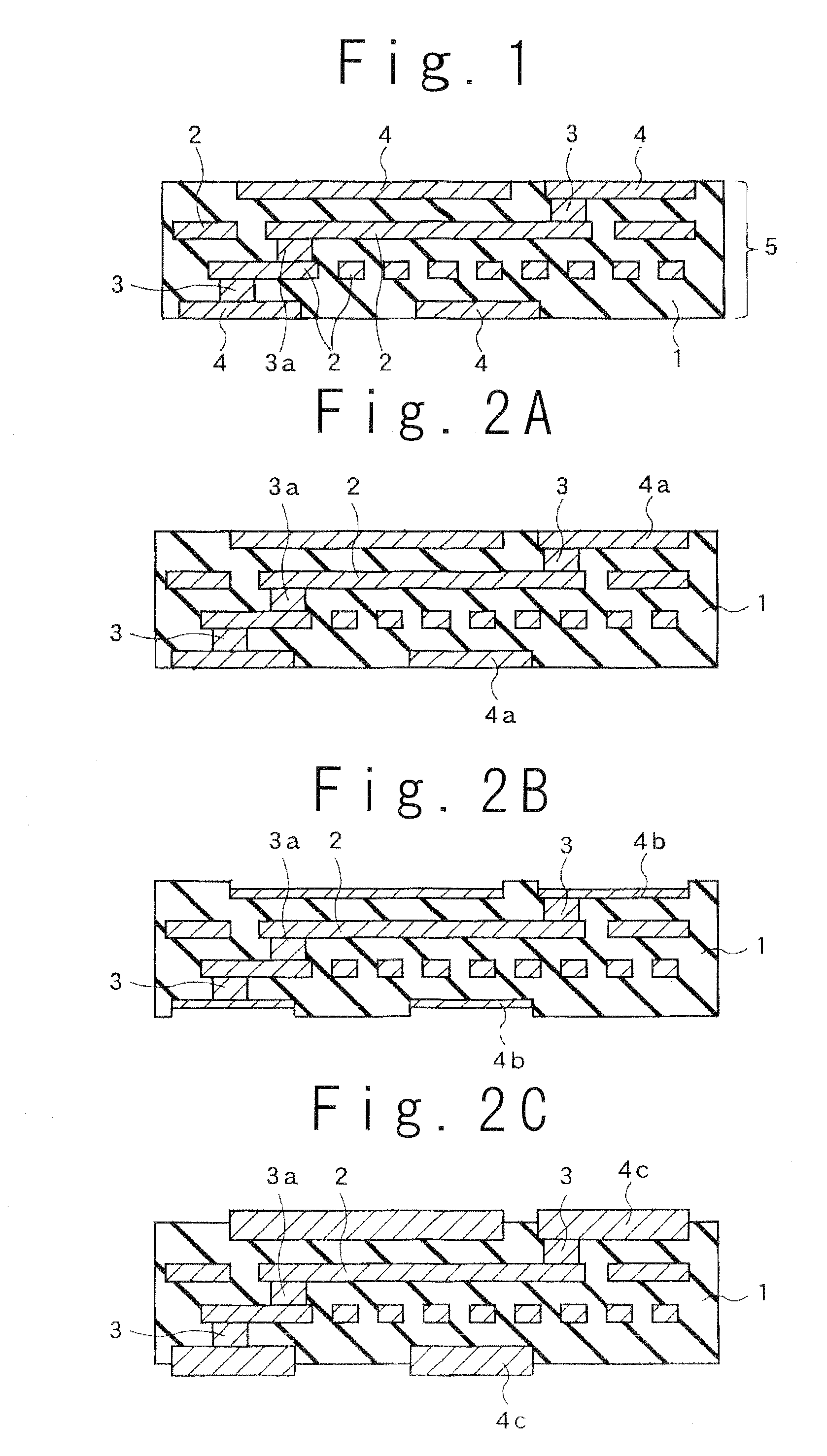
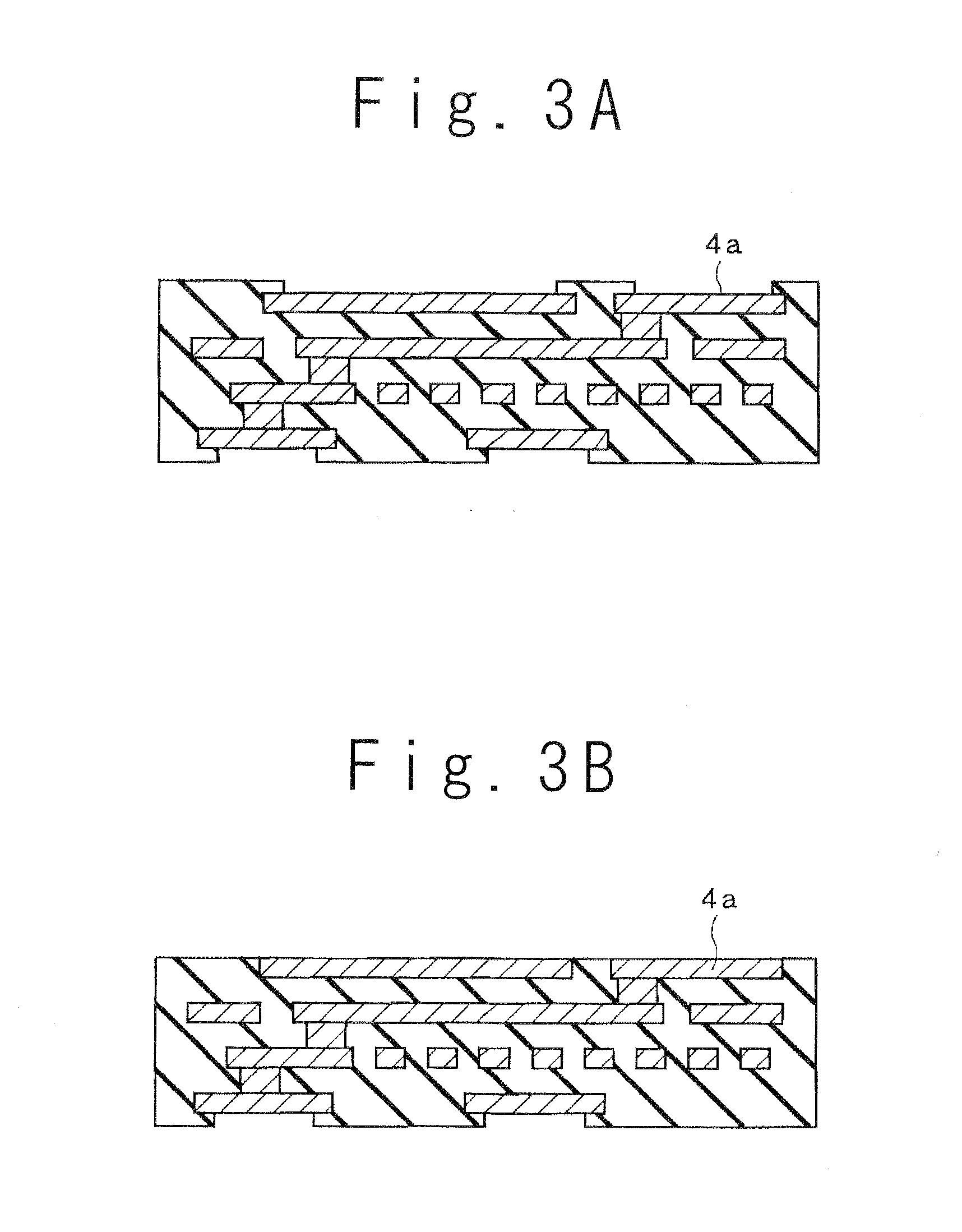
[0150]Exemplary embodiments of the present invention will be described in detail below with reference to the attached drawings. First, a first exemplary embodiment of the present invention will be described with reference to FIG. 1. FIG. 1 is a cross-sectional view showing a wiring board for mounting semiconductor device according to the present exemplary embodiment. In the wiring board for mounting semiconductor device, 5 according to the present exemplary embodiment, upper and lower wirings 2 and a via 3a for electrically connecting the upper and lower wirings 2 are provided in a dielectric film 1, and electrode pads 4 are provided to both the front and back surfaces of the wiring board for mounting semiconductor device, 5, namely, to both the front and back surfaces of the dielectric film 1. At least portion of the lateral side of the electrode pad 4 is buried in the dielectric film 1 and the wiring 2 and the electrode pad 4 are connected through a via 3. The wiring board for mou...


PUM


Abstract

A wiring board for mounting semiconductor device, includes at least a dielectric film 1; wirings formed in the dielectric film 1; a plurality of electrode pads provided at front and back surfaces of the dielectric film with their surfaces exposed and at least portions of lateral sides of them buried into the dielectric film; vias connecting the wirings and the electrode pads. At least one via connecting each other the wirings formed in the dielectric film includes second material different from first material forming the vias connecting the wirings and the electrode pads. The wiring board for mounting semiconductor device, is effective for an increase in terminals and finer pitch of terminal intervals due to an improvement in integration, performance or multi-function of semiconductor devices, can mount semiconductor devices especially on both sides of the board at a high density and high accuracy, and furthermore, is excellent in reliability as well.

Description

TECHNICAL FIELD[0001]The present invention relates to a wiring board for mounting semiconductor device, a manufacturing method of the same, and a wiring board assembly using the wiring board, and in particular, relates to a wiring board for mounting semiconductor device, which can provide a high performance and high reliability wiring board assembly and module, and a manufacturing method of the same, and a wiring board assembly using the wiring board.BACKGROUND ART[0002]Recently, as semiconductor devices get higher integrated, higher performance, and larger number of functions, the number of the terminals increases and the pitch between the terminals becomes narrower. As for a wiring board for mounting such semiconductor devices, it is required to mount semiconductor devices at a higher density and higher accuracy, and to be more excellent in reliability than before. Examples of the wiring board for mounting semiconductor devices often used currently include a build-up board which i...

Claims


Application Information

Patent Timeline
IPC IPC(8): H05K1/11H05K1/18
CPCH01L21/6835H01L23/49811H01L2924/12041H01L2224/45144H01L24/48H01L2924/01327H05K2203/061H01L23/49822H01L23/49827H01L23/49833H01L23/49866H01L2221/68345H01L2221/68359H01L2224/16225H01L2224/48091H01L2224/48227H01L2924/01078H01L2924/01079H01L2924/09701H01L2924/15311H01L2924/15312H01L2924/1532H01L2924/19041H05K1/115H05K1/117H05K3/20H05K3/4614H05K3/4682H05K3/4694H05K2201/0272H05K2201/0352H05K2201/09845H05K2201/09972H05K2203/0425H01L2924/00014H01L2924/00H01L24/45H01L2224/05599
Inventor FUNAYA, TAKUOMURAI, HIDEYAYAMAMICHI, SHINTAROKIKUCHI, KATSUMIHONDA, HIROKAZUMIYAZAKI, SHINICHI
Owner RENESAS ELECTRONICS CORP
Why Eureka
Try Eureka