
Semiconductor memory device and method of fabricating the same

a memory device and semiconductor technology, applied in semiconductor devices, digital storage, instruments, etc., can solve the problems of poor reliability of insulating film, high write and read voltage, and difficulty in fabricating a large capacity memory

Inactive Publication Date: 2009-02-26
FUJITSU LTD
View PDF2 Cites 22 Cited by
  • Summary
  • Abstract
  • Description
  • Claims
  • Application Information

AI Technical Summary

Problems solved by technology

In other words, in the 1T1C FeRAM, it is difficult to fabricate a large capacity memory.
However, in the current FET FeRAM, write and read voltages are high, and the reliability of the insulating film is poor.
On this account, the FET FeRAM is not commercially available yet.
However, in such a method, the properties and reliability of the ferroelectric film and the ferromagnetic film might be impaired.

Method used


Image

  • Semiconductor memory device and method of fabricating the same
  • Semiconductor memory device and method of fabricating the same
  • Semiconductor memory device and method of fabricating the same

Examples


first embodiment

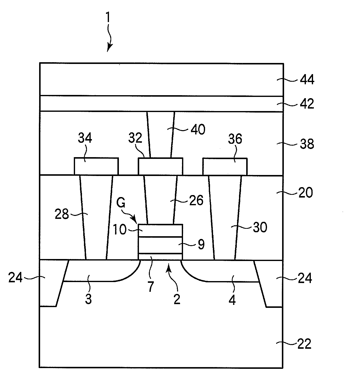
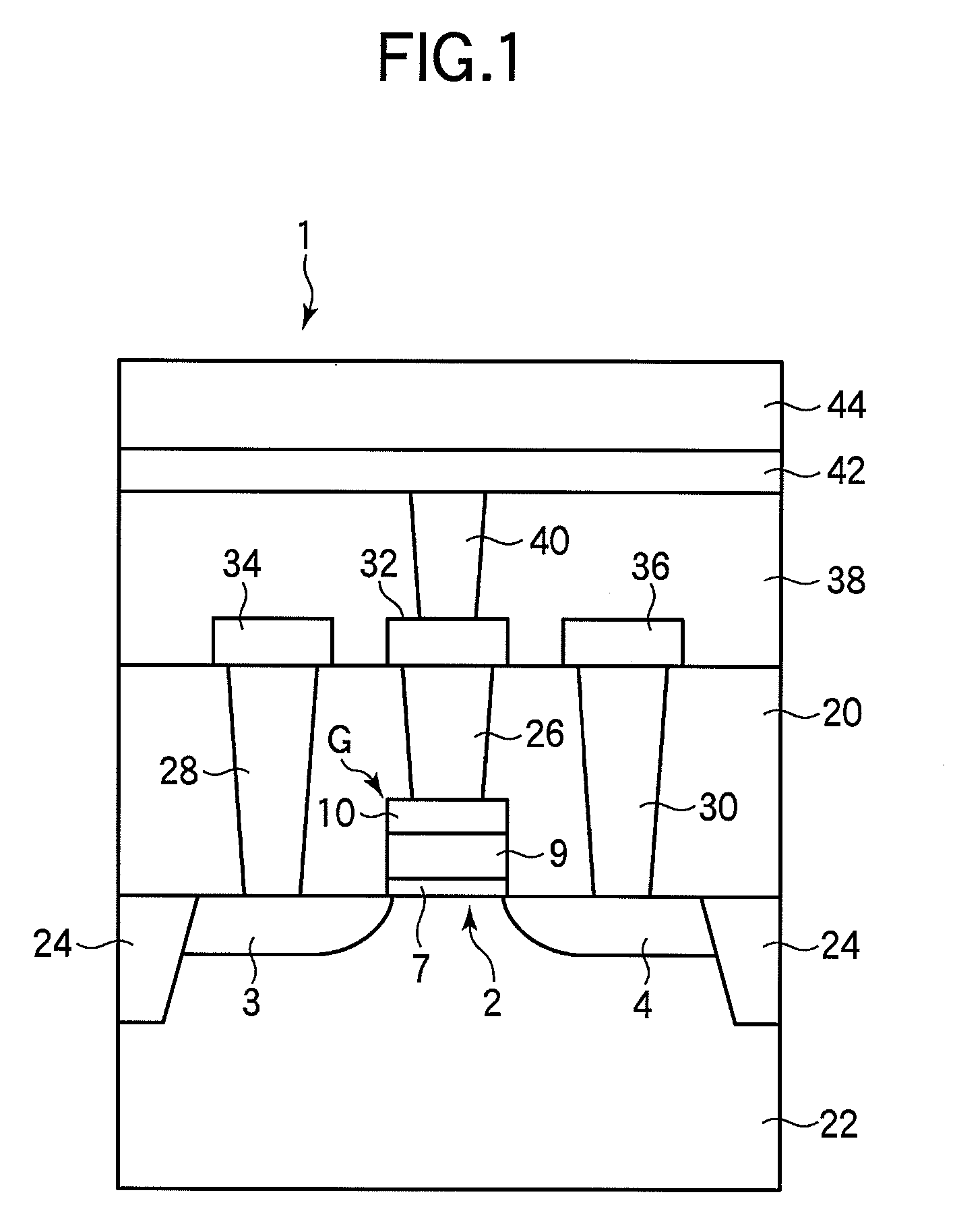
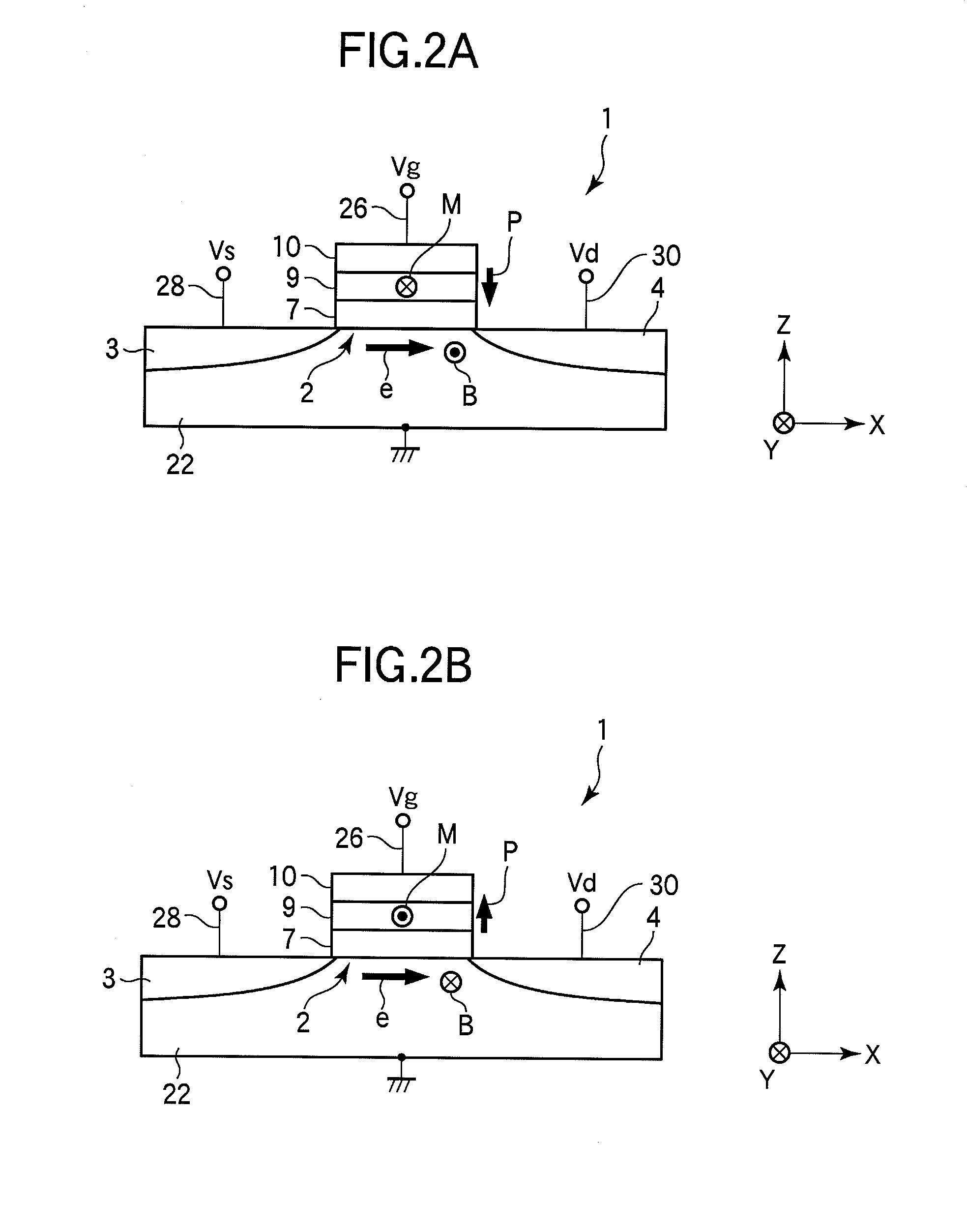
[0024]A semiconductor memory device and a method of fabricating the same according to a first embodiment of the invention will be described with reference to FIG. 1 to FIGS. 4A and 4B. The semiconductor memory device 1 according to the embodiment has the structure similar to that of the MFIS FeRAM, which is characterized in that a multiferroic film is used in the ferroelectric film (F). The multiferroic film exhibits ferroelectricity (ferroelectric property) as well as ferromagnetism (ferromagnetic property). The multiferroic film has the property that when one of the electric field and the magnetic field is changed, the other one's characteristic is altered. In the embodiment, such a multiferroic film is used that the orientation of dielectric polarization is nearly orthogonal to the orientation of magnetization.

[0025]FIG. 1 shows the cross sectional structure vertical to the substrate surface of the semiconductor memory device 1. As shown in FIG. 1, for example, the semiconductor ...

second embodiment

[0068]A semiconductor memory device and a method of fabricating the same according to a second embodiment of the invention will be described with reference to FIG. 5 to FIGS. 7A and 7B. A semiconductor memory device 1 according to the embodiment also has the structure similar to the MFIS FeRAM, which is characterized in that a multiferroic film is used for the ferroelectric film (F). First, the schematic configuration of the semiconductor memory device according to the embodiment will be described with reference to FIGS. 5 and 6. FIG. 5 shows a perspective view schematically depicting the structure of the semiconductor memory device 1 according to the embodiment. FIG. 6 shows a schematic diagram depicting the semiconductor memory device 1 shown in FIG. 5 seen in the normal direction of the substrate surface. Among the components of the semiconductor memory device 1 according to the embodiment, the components having functions and operations similar to those of the semiconductor memor...

third embodiment

[0095]A semiconductor memory device and a method of fabricating the same according to a third embodiment of the invention will be described with reference to FIGS. 8 and 9. A semiconductor memory device 1 according to the embodiment also has the structure similar to the MFIS FeRAM, which is characterized in that a multiferroic film is used for the ferroelectric film (F). FIG. 8 shows a perspective view schematically depicting the structure of the semiconductor memory device 1 according to the embodiment. FIG. 9 shows a schematic diagram depicting a cross section of a channel region 2 of the semiconductor memory device 1 shown in FIG. 8 cut in the direction in parallel with the channel width.

[0096]For easy understanding, an XYZ rectangular coordinates system is used to provide discussions. In FIGS. 8 and 9, an XY-plane is taken in parallel with the substrate surface of a semiconductor substrate 22. The X-axis is in parallel with the channel length direction of the channel region 2, a...


PUM


Abstract

The present invention is to provide a semiconductor memory device capable of providing excellent storage properties, scaling and high integration and a method of fabricating the same. A semiconductor memory device has a multiferroic film exhibiting ferroelectricity and ferromagnetism, a channel region on an interface of a semiconductor substrate below the multiferroic film, source and drain regions formed on both sides of the channel region, a gate electrode (data write electrode) applying gate voltage to the multiferroic film to write data in such a way that the orientation of magnetization is changed as corresponding to the orientation of dielectric polarization, and source and drain electrodes (data read electrodes) that read data based on a deviation in a flow of the carrier, the deviation caused by applying the Lorentz force to the carrier flowing in the channel region from a magnetic field occurring in the channel region because of magnetization.

Description

CROSS REFERENCE TO RELATED APPLICATIONS[0001]This application is a Continuation of International Application No. PCT / JP2006 / 306496, with an international filing date of Mar. 29, 2006, which designating the United States of America, the entire contents of which are incorporated herein by reference.BACKGROUND OF THE INVENTION[0002]1. Field of the Invention[0003]The present invention relates to a semiconductor memory device and a method of fabricating the same.[0004]2. Description of the Related Art[0005]A non-volatile random access memory (RAM) that maintains last data even though a power supply is turned off and allows random access is regarded as a promising device that forms the foundation of the ubiquitous society in the fields of personal identification and security.[0006]Among various non-volatile RAMs, a non-volatile memory (FeRAM) that uses a ferroelectric having spontaneous polarization in the dielectric layer of a capacitor is expected as the next generation memory in the fi...

Claims


Application Information

Patent Timeline
Patent Type & Authority Applications(United States)
IPC IPC(8): H01L27/115H01L21/8246
CPCG11C11/22H01L21/28291H01L29/78391H01L29/6684H01L43/06H01L29/516H01L29/40111H10N52/00
Inventor MARUYAMA, KENJIKONDO, MASAOSATO, KEISUKE
Owner FUJITSU LTD
Learn More