Multilayer ceramic electronic device and method for manufacturing the same

a multi-layer ceramic and electronic device technology, applied in the field of electronic devices, can solve the problems of difficult to satisfactorily meet the demands of protruding electrodes and prevent the mounting of high-density electronic devices on the surface, and achieve the effects of improving miniaturization, high reliability, and outstanding impact resistan

Active Publication Date: 2009-03-05
MURATA MFG CO LTD
View PDF24 Cites 26 Cited by
  • Summary
  • Abstract
  • Description
  • Claims
  • Application Information

AI Technical Summary

Benefits of technology

[0014]To overcome the problems described above, preferred embodiments of the present invention provide a method for manufacturing a multilayer ceramic electronic device, wherein leakage of an underfill resin arranged to fix a surface mount electronic device does not

Problems solved by technology

Therefore, it is difficult to satisfactorily meet the demands for protruding electrodes (columnar electrodes) 63 having smaller diameters and high aspect ratios.
However, the resin leaks from a lower region of the semiconducto

Method used


Image

  • Multilayer ceramic electronic device and method for manufacturing the same
  • Multilayer ceramic electronic device and method for manufacturing the same
  • Multilayer ceramic electronic device and method for manufacturing the same

Examples


first preferred embodiment

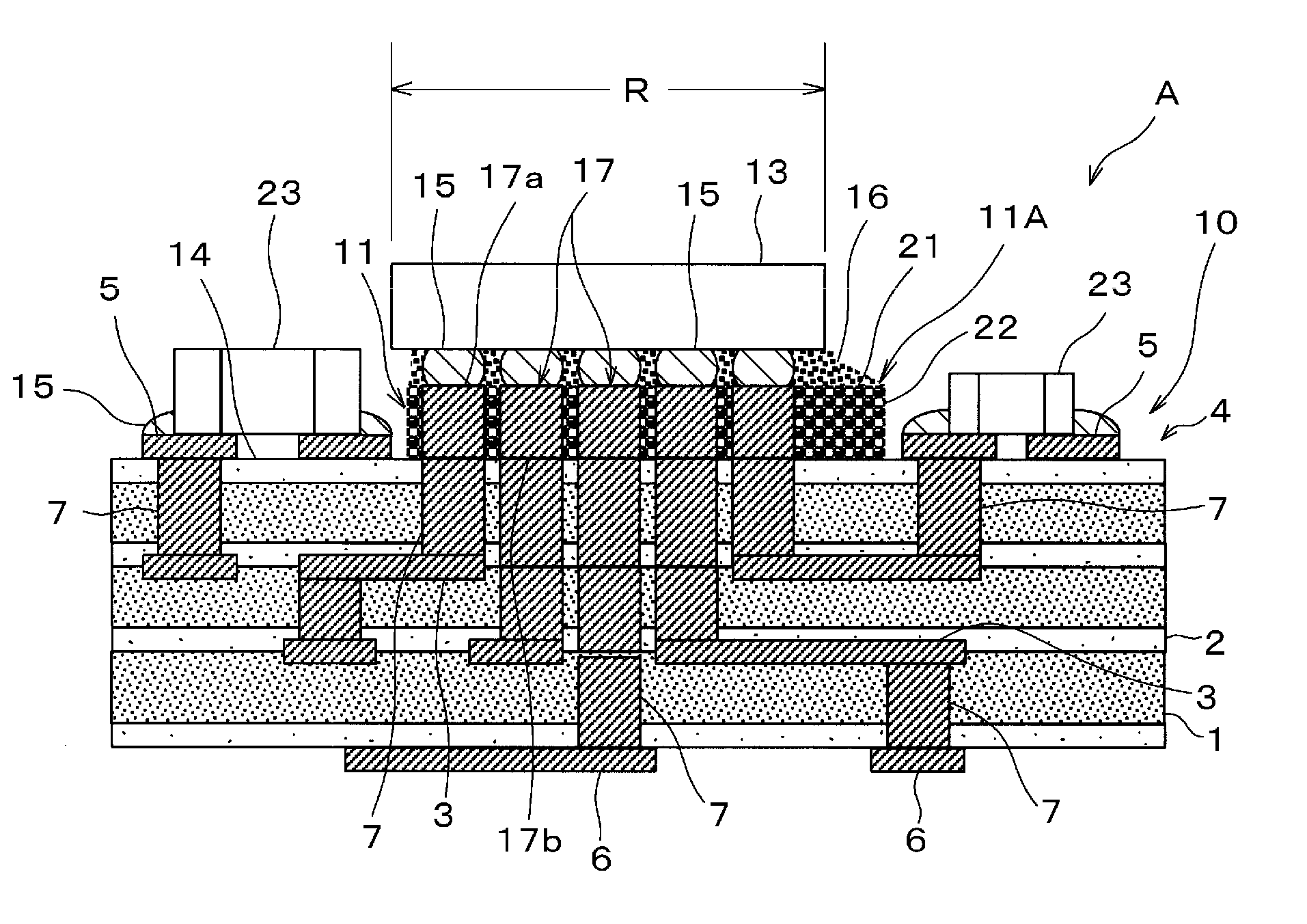
[0084]FIG. 1 is a sectional view showing the entire structure of a multilayer ceramic electronic device according to a preferred embodiment of the present invention.

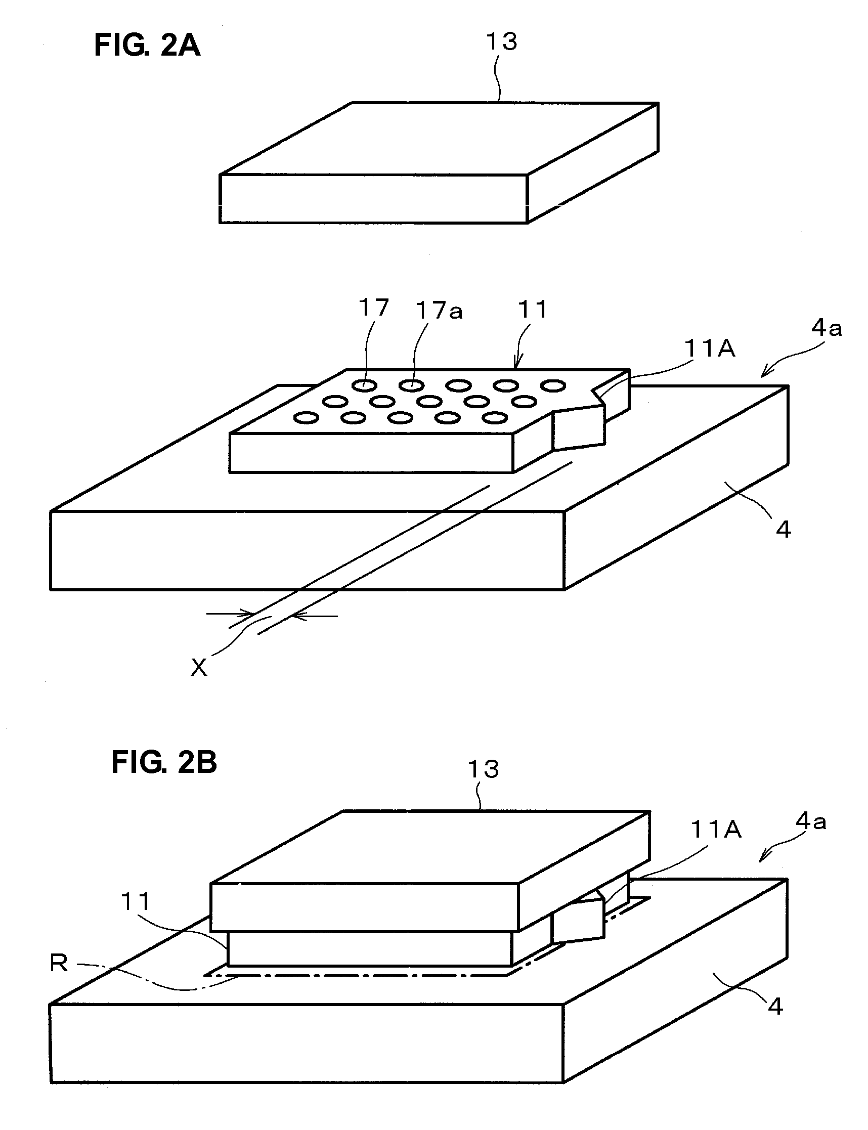
[0085]Furthermore, FIG. 2A is an exploded perspective view showing a portion (arrangement of a seat portion on a multilayer ceramic element assembly) of the multilayer ceramic electronic device shown in FIG. 1, and FIG. 2B is a perspective view showing a state in which a semiconductor element is mounted on the seat portion. In FIGS. 2B and 2B, only the multilayer ceramic element assembly, the seat portion, and the semiconductor element are shown, and the other elements are omitted.

[0086]As shown in FIGS. 1 to 2B, a multilayer ceramic electronic device A according to the first preferred embodiment of the present invention includes a multilayer ceramic element assembly 4 including first ceramic layers 1 which define ceramic base material layers, second ceramic layers 2 which define shrinkage restriction layers which are la...


PUM

PropertyMeasurementUnit
Thicknessaaaaaaaaaa
Thicknessaaaaaaaaaa
Temperatureaaaaaaaaaa

Abstract

In a method for manufacturing a multilayer ceramic electronic device, a resin introduction portion located outside a vertically projected region of a surface mount electronic device is disposed on a seat portion which includes a non-metallic inorganic powder as a primary component and on which the surface mount electronic device, e.g., a semiconductor element, is mounted, and a resin is supplied to the resin introduction portion so as to fill the resin into the seat portion and a gap between the seat portion and a multilayer ceramic element assembly. Unsintered ceramic base material layers and shrinkage restriction layers arranged to restrict shrinkage of the unsintered ceramic base material layers in a direction substantially perpendicular to a thickness direction of the unsintered ceramic base material layers are laminated and, thereby, an unfired multilayer ceramic element assembly is formed, which does not shrink in a direction substantially perpendicular to a lamination direction in a firing step.

Description

BACKGROUND OF THE INVENTION[0001]1. Field of the Invention[0002]The present invention relates to an electronic device and a method for manufacturing the same. In particular, the present invention relates to a multilayer ceramic electronic device in which a surface mount electronic device is mounted on a multilayer ceramic element assembly and a method for manufacturing the same.[0003]2. Description of the Related Art[0004]In recent years, performance of electronic devices in the electronics field has improved significantly and contributed to increased information processing speeds, miniaturization of apparatuses, and expansion in functionality of information processing apparatuses, e.g., large-scale computers, mobile communication terminals, and personal computers.[0005]A multi-chip module (MCM) in which a plurality of semiconductor devices, e.g., very large scale integrations (VLSIs) and ultra large scale integrations (ULSIs), are mounted on a ceramic substrate has been used for su...

Claims


Application Information

Patent Timeline
IPC IPC(8): H05K1/03H05K3/00
CPCH01L21/4857Y10T29/49126H01L23/15H01L23/49822H01L24/16H01L2224/13099H01L2924/01002H01L2924/01004H01L2924/01013H01L2924/01027H01L2924/01029H01L2924/01033H01L2924/0104H01L2924/01046H01L2924/01056H01L2924/01074H01L2924/01079H01L2924/01082H01L2924/09701H01L2924/14H01L2924/19041H01L2924/19042H01L2924/19043H01L2924/19105H01L2924/30107H05K1/0306H05K3/305H05K3/4626H05K3/4629H05K2201/0116H05K2201/10378H05K2201/10674H05K2201/10977H05K2203/1147H01L2224/16225H01L2224/73204H01L2924/01005H01L2924/01006H01L2924/01047H01L2924/014H05K1/181H01L2224/16235Y10T29/49146Y10T29/4913H01L23/13H01L2924/15787H01L2924/12042Y02P70/50H01L2924/00
Inventor NOMIYA, MASATOSAKAI, NORIONISHIDE, MITSUYOSHI
Owner MURATA MFG CO LTD
Why Eureka
Try Eureka