Supercharge Your Innovation With Domain-Expert AI Agents!

Semiconductor device and method of fabricating metal gate of the same

a technology of semiconductor devices and semiconductor devices, which is applied in the direction of semiconductor devices, semiconductor/solid-state device details, electrical apparatus, etc., can solve the problems of leakage current increase, metal gate is also believed, power consumption of cmos devices exceeding a standard value, etc., and achieves low sheet resistance characteristics.

Active Publication Date: 2009-03-12
SAMSUNG ELECTRONICS CO LTD
View PDF4 Cites 26 Cited by
  • Summary
  • Abstract
  • Description
  • Claims
  • Application Information

AI Technical Summary

Benefits of technology

[0009]To address the above and/or other problems, the present invention provides a method of fabricating semiconductor device, in particu

Problems solved by technology

Thus, as the thickness of the conventional SiO2 thin film used as a gate insulating film is reduced, the leakage current is increased due to tunneling, and thus, power consumption of the CMOS device exceeds a standard value.
The metal gate is also believed to decrease the high sheet resistance problem of conventional polysilicon.
However, if a pure metal is used to obtain low sheet resistance, the diffusion problem still remains.
However, TiN and TaN are easily oxidized since TiN and TaN are highly oxidative.
Also, problems of thermal stability and diffusion into the gate insulating film still remain.

Method used


Image

  • Semiconductor device and method of fabricating metal gate of the same
  • Semiconductor device and method of fabricating metal gate of the same
  • Semiconductor device and method of fabricating metal gate of the same

Examples


Embodiment Construction

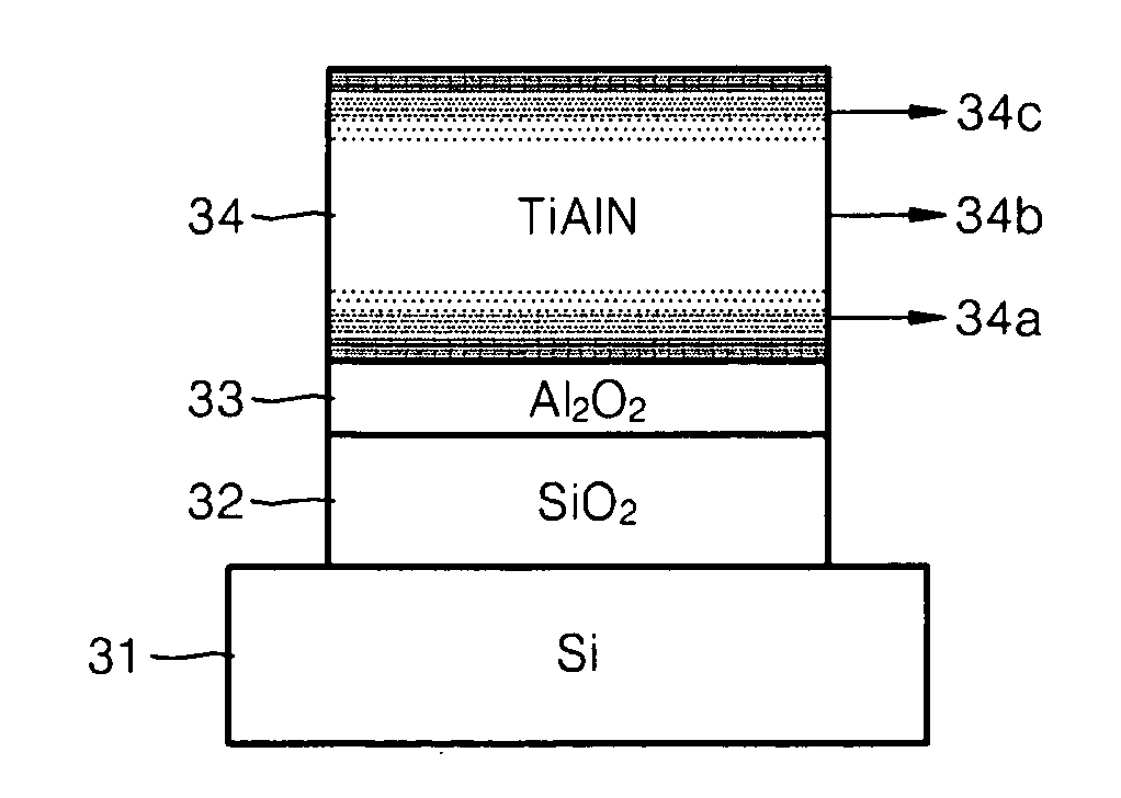
[0028]A semiconductor device that includes a metal gate having a low sheet resistance characteristic and a diffusion barrier characteristic according to the present invention and a method of fabricating the metal gate of the semiconductor device will now be described more fully with reference to the accompanying drawings in which exemplary embodiments of the invention are shown.

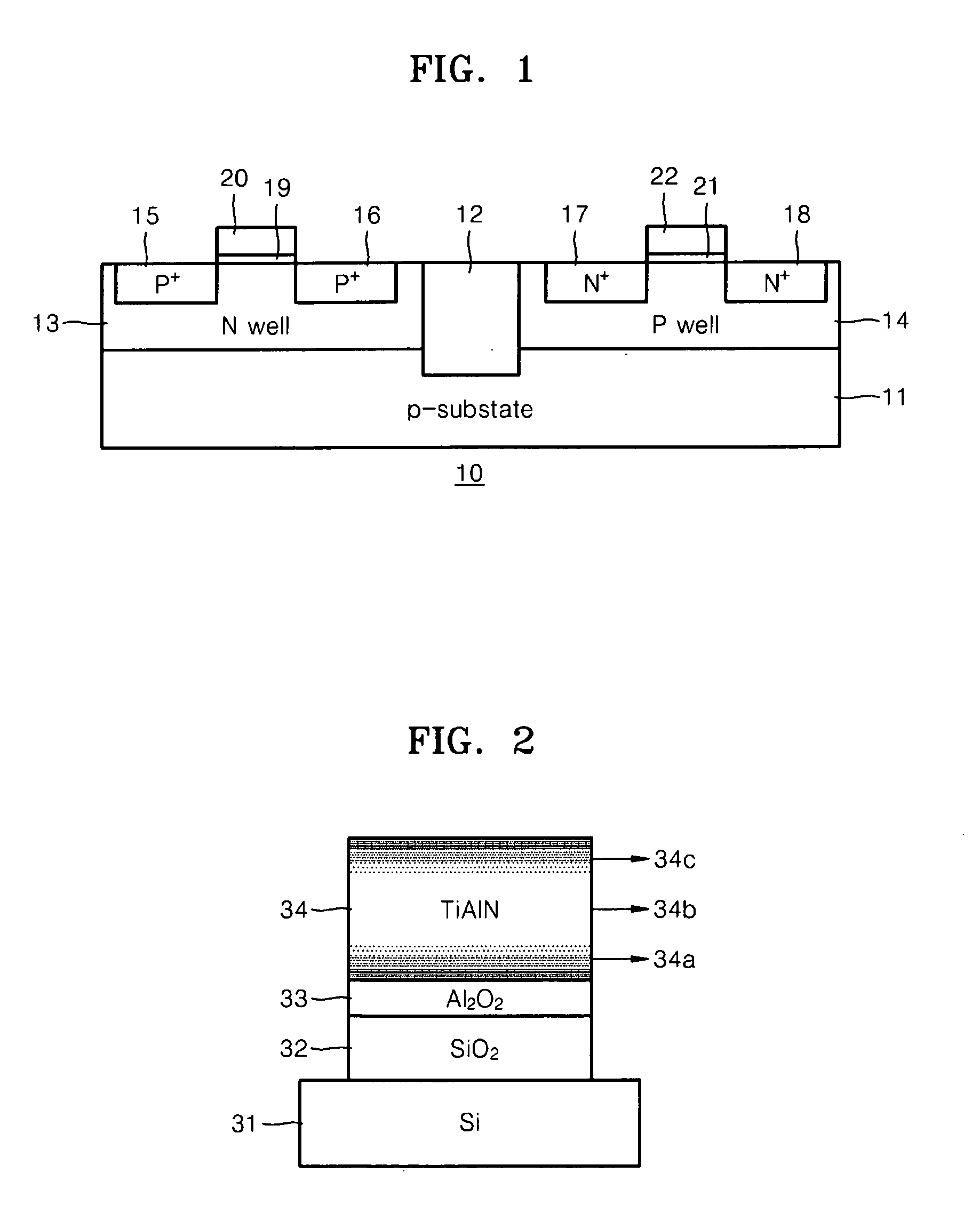
[0029]FIG. 1 is a schematic cross-sectional view of the structure of a complementary metal oxide semiconductor (CMOS) device 10 that includes a p-channel metal oxide semiconductor (PMOS) transistor and an n-channel metal oxide semiconductor (NMOS) transistor. Referring to FIG. 1, the CMOS device 10 includes a PMOS transistor and an NMOS transistor respectively formed on a P-type substrate 11. In FIG. 1, the PMOS transistor is depicted in a left side of the drawing and the NMOS transistor is depicted in a right side of the drawing. A field oxide film 12 is formed between the PMOS transistor and the NMOS transi...


PUM


Abstract

Provided is a semiconductor device that comprises a metal gate having a low sheet resistance characteristic and a high diffusion barrier characteristic and a method of fabricating the metal gate of the semiconductor device. The semiconductor device includes a metal gate formed on a gate insulating film, wherein the metal gate is formed of a metal nitride that contains Al or Si and includes upper and lower portions where the content of Al or Si is relatively high and a central portion where the content of Al or Si is relatively low.

Description

CROSS-REFERENCE TO RELATED PATENT APPLICATION[0001]This application claims the benefit of Korean Patent Application No. 10-2007-0090553, filed on Sep. 6, 2007, in the Korean Intellectual Property Office, the disclosure of which is incorporated herein in its entirety by reference.BACKGROUND OF THE INVENTION[0002]1. Field of the Invention[0003]The present invention relates to a semiconductor device and a method of fabricating a metal gate of the semiconductor device, and more particularly, to a complementary metal oxide semiconductor (CMOS) device having a low sheet resistance characteristic and a high diffusion barrier characteristic and a method of fabricating a metal gate of the CMOS device.[0004]2. Description of the Related Art[0005]A complementary metal oxide semiconductor (CMOS) device formed to be complementarily operated includes a p-channel metal oxide semiconductor (PMOS) transistor and an n-channel metal oxide semiconductor (NMOS) transistor. Such CMOS devices have increas...

Claims


Application Information

Patent Timeline
IPC IPC(8): H01L21/8238H01L27/092
CPCH01L21/28088H01L21/823828H01L29/517H01L29/513H01L29/4966H01L21/18H01L21/8238
Inventor PARK, SUNG-HONOH, JIN-SEOJEON, JOONG S.
Owner SAMSUNG ELECTRONICS CO LTD
Features
  • R&D
  • Intellectual Property
  • Life Sciences
  • Materials
  • Tech Scout
  • Unparalleled Data Quality
  • Higher Quality Content
  • 60% Fewer Hallucinations
Learn More