Flash memory device and method of operating the same

a flash memory and memory cell technology, applied in the field of flash memory devices, can solve problems such as the malfunction of memory cells

Active Publication Date: 2009-03-12
SK HYNIX INC
View PDF1 Cites 36 Cited by
  • Summary
  • Abstract
  • Description
  • Claims
  • Application Information

AI Technical Summary

Benefits of technology

[0009]In the flash memory device and the method of operating the same disclosed in the present invention, the conditions of the voltage (or the current) applied during the reading operation are differently adjusted according to an accumulated number of times of a programming operation, an erasing operation or a reading operation (the accumulated number of operation cycle), and so even if a level of the threshold voltage is changed to a level which differs from that of the target voltage by an increase of the accumulated number of operation cycle regardless of the programming operation (or the erasing operation) being normally performed, the reliability of the reading operation can be enhanced to prevent a malfunction of the memory cell from being generated.
[0012]The bit line current control unit controls an extent of turning on of the switching element to lower a value of the reference current as the number of times of erasing is increased.
[0017]The method of operating the flash memory device according to the second embodiment of the present invention further comprises the step of increasing the number of times of an erasing operation after performing the erasing operation.
[0023]The method of operating a flash memory device according to the fourth embodiment of the present invention further comprises the step of increasing the number of times of erasing after performing the erasing operation.

Problems solved by technology

If the threshold voltage is changed under the same conditions of the programming operation, the data stored in the memory cell is not read normally when the reading operation is performed, causing a malfunction of the memory cell.

Method used


Image

  • Flash memory device and method of operating the same
  • Flash memory device and method of operating the same
  • Flash memory device and method of operating the same

Examples


Embodiment Construction

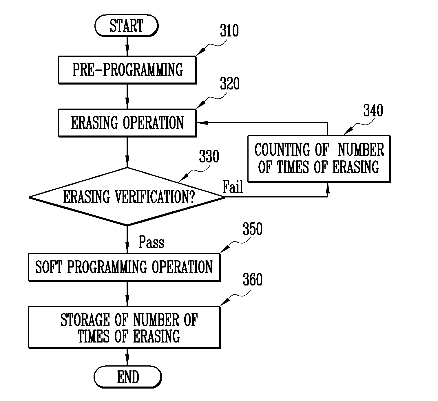
[0029]Hereinafter, the preferred embodiments of the present invention will be explained in more detail with reference to the accompanying drawings. However, the embodiments of the present invention may be modified variously and a scope of the present invention should not be limited to the below embodiments. The description herein is provided for illustrating more completely to those skilled in the art.

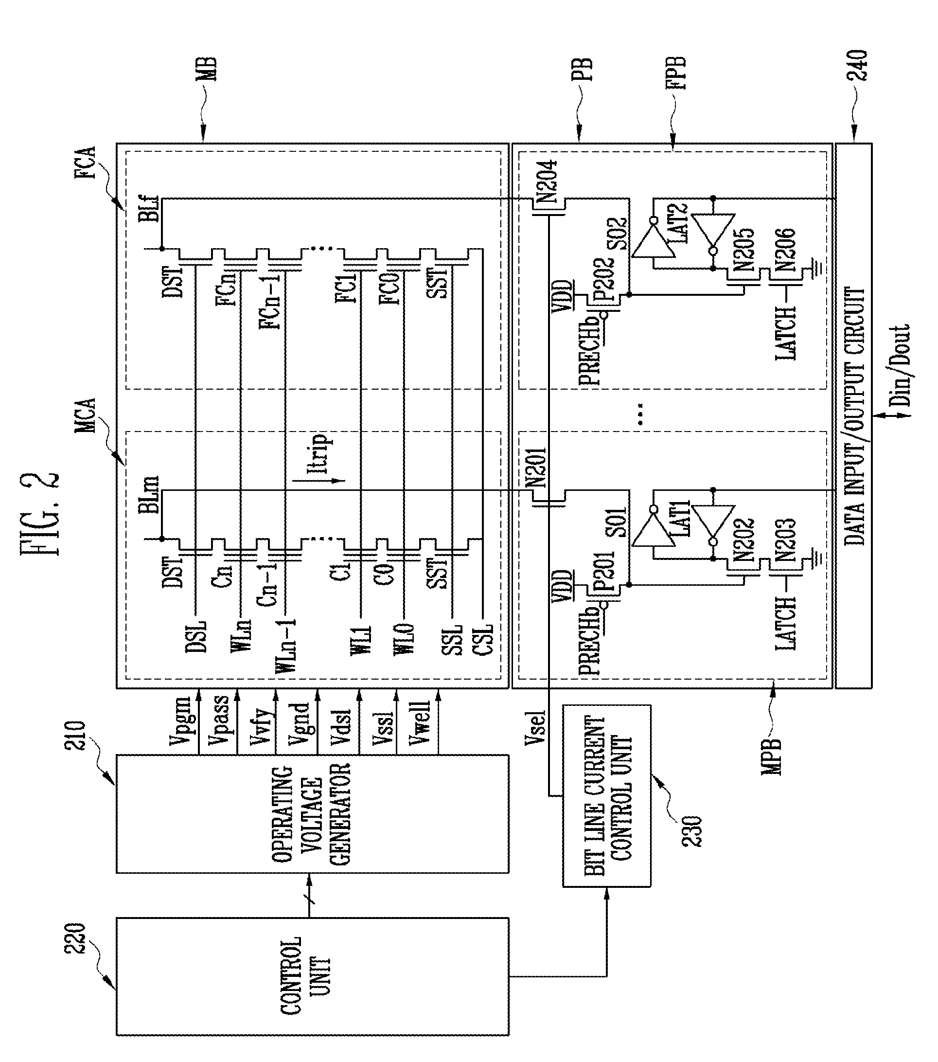
[0030]FIG. 2 is a circuit diagram for illustrating a flash memory device according to one embodiment of the present invention.

[0031]Referring to FIG. 2, a flash memory device according to one embodiment of the present invention comprises a memory cell array including a plurality of memory cell blocks MB (for convenience, only one cell block is shown in the drawing), a page buffer unit PB, an operating voltage generator 210, a control unit 220, a bit line current control unit 230 and a data input / output circuit 240.

[0032]The memory cell array includes a plurality of memory cell blocks M...


PUM


Abstract

A flash memory device and a method of operating the same is disclosed, in which the conditions of voltage (or current) applied during the reading operation are differently adjusted according to an accumulated number of times of a programming operation, an erasing operation or a reading operation (an accumulated number of operation cycle). Even if a level of the threshold voltage is changed to a level which differs from that of the target voltage by an increase of the accumulated number of operation cycle regardless of the programming operation (or the erasing operation) being normally performed, the reliability of the reading operation can be enhanced to prevent a malfunction of the memory cell from being generated.

Description

CROSS-REFERENCE TO RELATED APPLICATIONS[0001]The present application claims priority to Korean Patent Application No. 10-2007-91518, filed on Sep. 10, 2007, which is incorporated herein by reference in its entirety.BACKGROUND OF THE INVENTION[0002]The present invention relates to a flash memory device and a method of operating the same, more particularly, to a flash memory device and a method of operating the same being capable of compensating operating characteristics which change as the number of the operation increases.[0003]As one kind of the memory devices, a non-volatile memory device has a characteristic that data stored in the memory cells are not erased even if a power supply is turned off. A flash memory device is a typical non-volatile memory device. The flash memory device may be classified into a NOR flash memory device and a NAND flash memory device based on a structure of a memory cell array. A gate of the flash memory cell has a structure comprising a tunnel insulati...

Claims


Application Information

Patent Timeline
Patent Type & Authority Applications(United States)
IPC IPC(8): G11C16/16G11C16/34
CPCG11C16/0483G11C16/349G11C16/26G11C16/12G11C16/16G11C16/30G11C16/3404G11C16/3459
Inventor LEE, KEUN WOOKIM, KI SEOG
Owner SK HYNIX INC
Why Eureka
Try Eureka