Optical space communication reception circuit, optical space communication device, optical space communication system, and electronic device

Inactive Publication Date: 2009-03-12
SHARP KK
View PDF4 Cites 17 Cited by
  • Summary
  • Abstract
  • Description
  • Claims
  • Application Information

AI Technical Summary

Benefits of technology

[0041]The present invention is made in the view of the problems, and an object of the present invention is to provide an optical space communication reception circuit, an optical space communication device, an optical space communication sy

Problems solved by technology

Therefore, any communication speed mode having maximum communicable distanc

Method used


Image

  • Optical space communication reception circuit, optical space communication device, optical space communication system, and electronic device
  • Optical space communication reception circuit, optical space communication device, optical space communication system, and electronic device
  • Optical space communication reception circuit, optical space communication device, optical space communication system, and electronic device

Examples


first embodiment

[0084]One embodiment of the present invention is described below with reference to drawings.

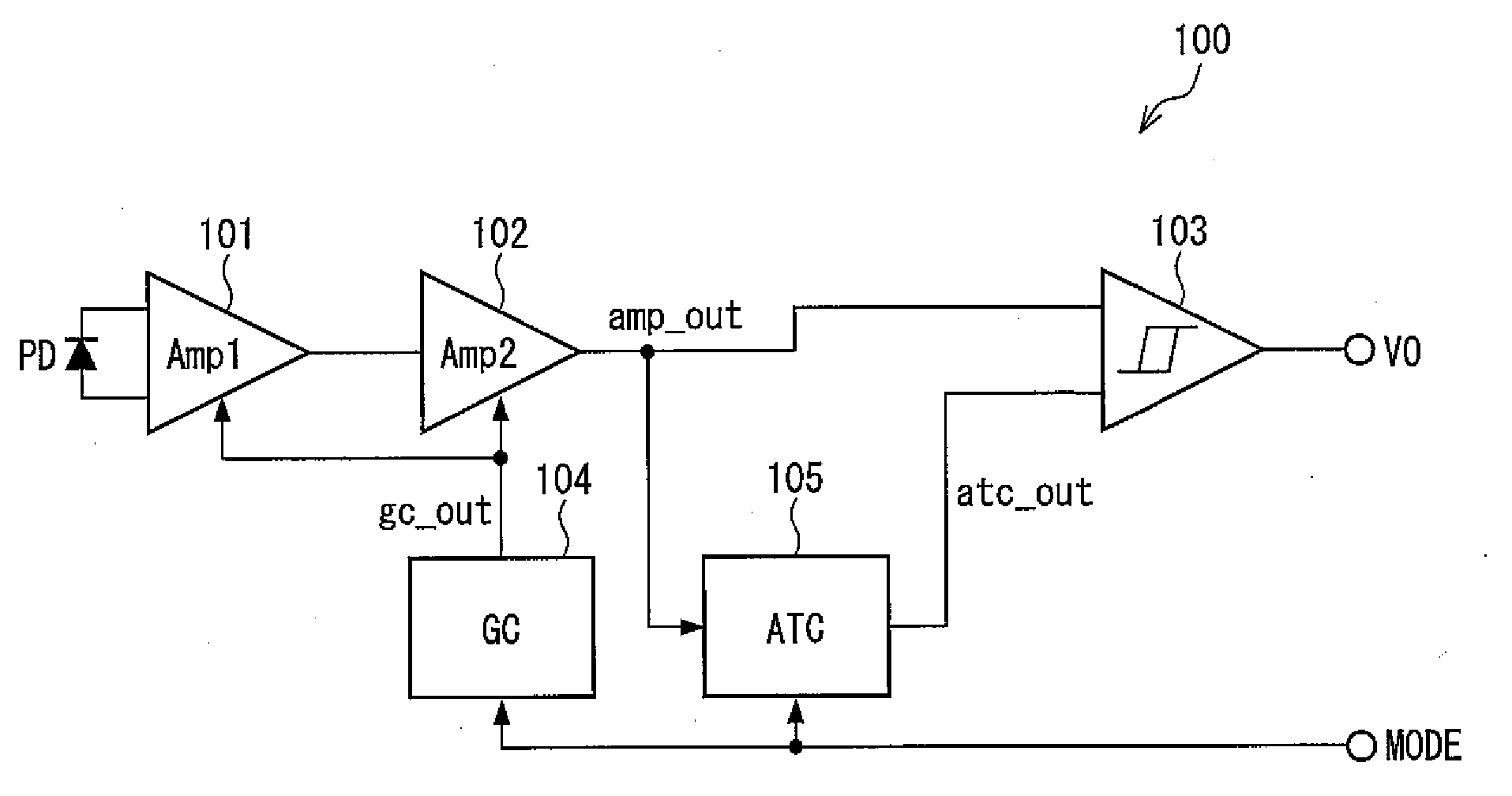
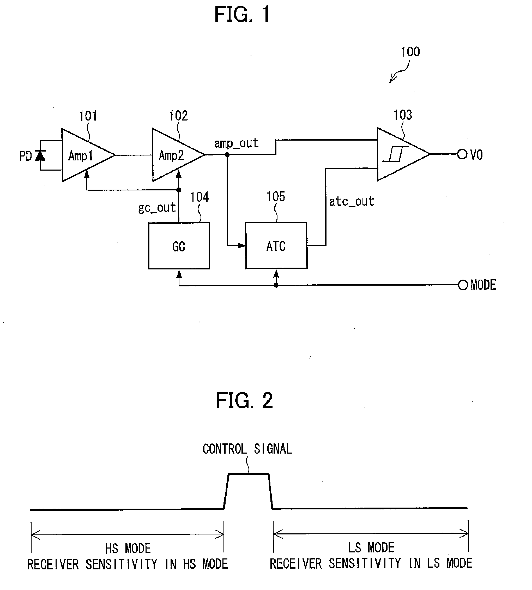
[0085]FIG. 1 is a block diagram of an equivalent circuit, showing an exemplary configuration of an optical space communication reception circuit 100 of the present embodiment.

[0086]As show in FIG. 1, the optical space communication reception circuit 100 of the present embodiment includes: a photo diode for outputting a received light signal as a current signal; a first amplifier (Amp 1) 101 for converting, into a voltage signal, the current signal outputted from the photo diode; a second amplifier (Amp 2) 102 for amplifying the voltage signal outputted from the first amplifier 101; a hysteresis comparator circuit 103 for comparing a voltage signalamp out outputted from the second amplifier 102 with a threshold valueatc out and outputting a pulse signal; a voltage output terminal (VO) connected to an output side of the hysteresis comparator circuit 103; a mode switch terminal (MODE) for receiv...

second embodiment

[0113]With reference to the drawings, the following description deals with another embodiment of the present invention. Configurations other than those described in the present embodiment are identical with the embodiment 1. For easy explanation, members having the same functions as those described in Embodiment 1 are given the same reference numerals in the present embodiment, and explanation thereof is omitted.

[0114]FIG. 5 is a block diagram of an equivalent circuit, showing an exemplary configuration of an optical space communication reception circuit 200 of the present embodiment.

[0115]As shown in FIG. 5, the optical space communication reception circuit 200 of the present embodiment is similar to a configuration of the optical space communication reception circuit 100 of the embodiment 1 except that a gain control circuit 104 is eliminated therefrom. In addition, the optical space communication reception circuit 200 of the present embodiment further includes a frequency control...

third embodiment

[0128]The following describes another embodiment of the present invention, with reference to the drawings. Note that configurations other than those described in the present embodiment are identical with the configurations of the Embodiments 1 and 2. Besides, for easy explanation, members having the same functions as those described in the drawings of the Embodiments 1 and 2 are given the same reference numerals in the present embodiment, and explanation thereof is omitted.

[0129]The Embodiments 1 and 2 describe the setting and the controlling for reducing noise influence without carrying out noise detection, presupposing that the devices are subject to the noise influence. However, the present embodiment describes an arrangement in which the noise is detected and then the noise influence is reduced according to the detected noise.

[0130]FIG. 8 shows a block diagram of an equivalent circuit, illustrating an exemplary configuration of an optical space communication reception circuit 30...


PUM


Abstract

An optical space communication reception circuit receives a signal in switched-over communication speed modes and under settings corresponding to the communication speed modes. Receiver sensitivity in the respective communication speed modes is set in advance such that maximum communicable distances in the communication speed modes are substantially equal. By this, it becomes possible, for example, in optical space transmission such as infrared communication and the like to enhance a false operation prevention characteristic against disturbance noise, without decreasing maximum communicable distances.

Description

[0001]This Nonprovisional application claims priority under 35 U.S.C. § 119(a) on Patent Application No. filed in Japan on May 31, 2007, the entire contents of which are hereby incorporated by reference.FIELD OF THE INVENTION[0002]The present invention relates to an optical space communication reception circuit, an optical space communication device, an optical space communication system, and an electronic device, and more particularly relates to art of reducing influence of disturbance noise in infrared communication.BACKGROUND OF THE INVENTION[0003]Optical space communication has become common due to adoption of infrared communication in portable phones or the like in recent years. The optical space communication is described below with reference to an embodiment in accordance with IrDA, a general code and standard for the infrared communication.[0004]FIG. 13 is a diagram schematically showing a configuration of a general infrared communication system. FIG. 13 shows a configuratio...

Claims


Application Information

Patent Timeline
IPC IPC(8): H04B10/06H04B10/114H04B10/11H04B10/2507
CPCH04B10/1141
Inventor YOKOGAWA, NARUICHINISHINO, TAKESHINAOE, HITOSHI
Owner SHARP KK
Why Eureka
Try Eureka