EPITAXIAL GROWTH OF THIN SMOOTH GERMANIUM (Ge) ON SILICON (Si) UTILIZING AN INTERFACIAL SILICON GERMANIUM (SiGe) PULSE GROWTH METHOD

a technology of interfacial silicon germanium and growth method, which is applied in the field of thin films, can solve the problems of uncontrolled growth during temperature ramps, and achieve the effects of reducing growth time and surface roughness

Inactive Publication Date: 2009-03-19
MASSACHUSETTS INST OF TECH
View PDF2 Cites 22 Cited by
  • Summary
  • Abstract
  • Description
  • Claims
  • Application Information

AI Technical Summary

Benefits of technology

[0008]The present invention provides for a method of growing thin and smooth germanium (Ge) on a strained silicon (Si) layer comprising the steps of: (a) treating surface of the strained Si layer to gaseous precursors of both Si (e.g., silane) and Ge (e.g., germane) for a predetermined short time duration Δt, where 1≦Δt≦30 seconds; and (b) depositing a thin Ge film on top of said treated Si layer, wherein said treatment step of (a) reduces growth time and surface roughness of the thin Ge film (e.g., sub-5 nm or sub-20 nm thick) deposited on the Si layer. In one embodiment, the treatment step (a) is conducted at a steady predetermined temperature T, where 450≦T≦900° C. In one embodiment, the predetermined short time duration Δt is chosen such that less than 10 A of SiGe is deposited.
[0009]The present invention provides for a method of growing thin and smooth germanium (Ge) on a relaxed silicon (Si) layer comprising the steps of: (a) treating surface of the relaxed Si layer to gaseous precursors o

Problems solved by technology

Brabant et al. do not teach or suggest a method for producing epitaxial structures with very thin layers of strained Si and Strained G

Method used


Image

  • EPITAXIAL GROWTH OF THIN SMOOTH GERMANIUM (Ge) ON SILICON (Si) UTILIZING AN INTERFACIAL SILICON GERMANIUM (SiGe) PULSE GROWTH METHOD
  • EPITAXIAL GROWTH OF THIN SMOOTH GERMANIUM (Ge) ON SILICON (Si) UTILIZING AN INTERFACIAL SILICON GERMANIUM (SiGe) PULSE GROWTH METHOD
  • EPITAXIAL GROWTH OF THIN SMOOTH GERMANIUM (Ge) ON SILICON (Si) UTILIZING AN INTERFACIAL SILICON GERMANIUM (SiGe) PULSE GROWTH METHOD

Examples


Embodiment Construction

[0022]While this invention is illustrated and described in a preferred embodiment, the invention may be produced in many different configurations. There is depicted in the drawings, and will herein be described in detail, a preferred embodiment of the invention, with the understanding that the present disclosure is to be considered as an exemplification of the principles of the invention and the associated functional specifications for its construction and is not intended to limit the invention to the embodiment illustrated. Those skilled in the art will envision many other possible variations within the scope of the present invention.

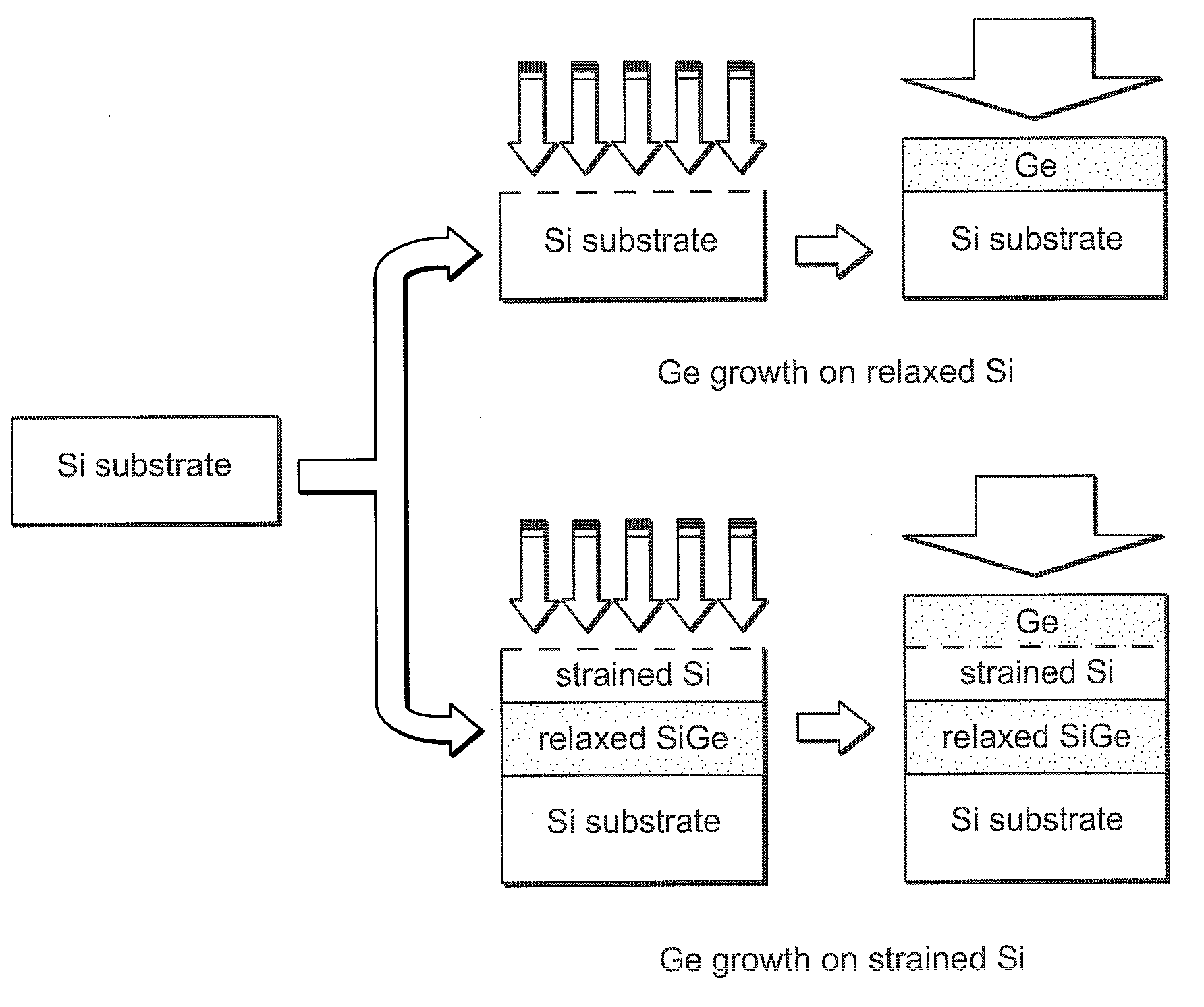
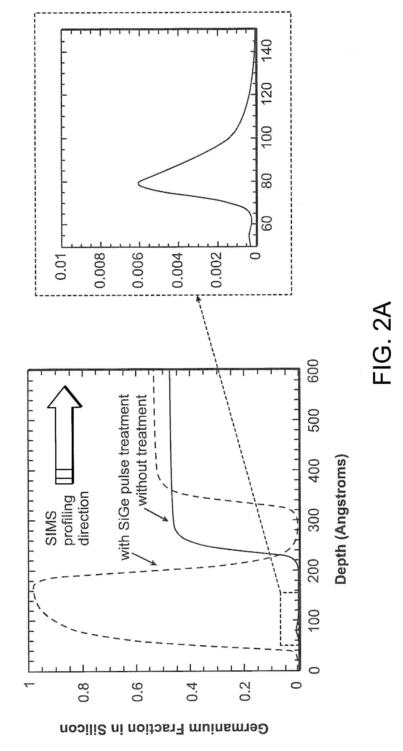
[0023]A method of interface treatment consisting of a short SiGe pulse is utilized to realize the growth of thin (e.g. 10 nm), smooth Ge films on Si. Such Ge films have a number of potential technological applications. For example, incorporating Ge into the channel of a MOSFET is one method to boost device performance and continue the progression to fu...


PUM


Abstract

Disclosed is a method of growing thin and smooth germanium (Ge) on a strained or relaxed silicon (Si) layer comprising the steps of: (a) treating surface of the strained or relaxed Si layer to gaseous precursors of both Si (e.g., silane) and Ge (e.g., germane) for a predetermined short time duration Δt, where 1≦Δt≦30 seconds; and (b) depositing a thin Ge film on top of said treated Si layer, wherein said treatment step of (a) reduces growth time and surface roughness of the thin Ge film (e.g., sub-5 nm or sub-20 nm thick) deposited on the Si layer. The treatment step (a) can be conducted at a steady predetermined temperature T, where 450≦T≦900° C. The predetermined short time duration Δt can be chosen such that less than 10 A of SiGe is deposited.

Description

PRIORITY INFORMATION[0001]This application claims priority from provisional application 60 / 973,226, filed Sep. 18, 2007 entitled, “Epitaxial Growth of Thin Smooth Germanium (Ge) on Silicon (Si) Utilizing an Interfacial Silicon Germanium (SiGe) Pulse Growth Method”, which is incorporated herein by reference in its entirety.BACKGROUND OF THE INVENTION[0002]1. Field of Invention[0003]The present invention relates generally to the field of thin films. More specifically, the present invention is related to the epitaxial growth of thin and smooth Germanium (Ge) on Silicon (Si) utilizing an interfacial Silicon Germanium (SiGe) pulse growth method.[0004]2. Discussion of Prior Art[0005]The paper to Lee et al. entitled, “Strained Ge channel p-type metal-oxide-semiconductor field-effect transistors grown in Si1-xGex / Si virtual substrates” teaches a method for growing Germanium (Ge) on thick Silicon Germanium (SiGe). Specifically, Lee et al. disclose a Ge MOSFET structure having a Ge layer form...

Claims


Application Information

Patent Timeline
IPC IPC(8): H01L29/165H01L21/205
CPCH01L21/02381H01L21/0245H01L21/02502H01L21/0251H01L29/78H01L21/0262H01L21/02658H01L29/1054H01L21/02532
Inventor GOMEZ, LEONARDOKIM, MEEKYUNGHOYT, JUDY L.
Owner MASSACHUSETTS INST OF TECH
Why Eureka
Try Eureka