RFID tag

a technology of rfid tags and ic chips, which is applied in the direction of burglar alarms, mechanical actuation of burglar alarms, and the removal of hand-held items, etc., can solve the problems of reducing the production volume of rfid tags, affecting the mutual flow of current, and increasing the cost of rfid tags, so as to reduce the manufacturing cost of rfid tags, eliminate the need for contact between antennas and ic chips, and reduce the cost of r

Active Publication Date: 2009-03-26
SES RFID SOLUTIONS
View PDF5 Cites 16 Cited by
  • Summary
  • Abstract
  • Description
  • Claims
  • Application Information

AI Technical Summary

Benefits of technology

[0007]In the conventional setting and connection method by electric connection, fine and mutually close connection terminals on an IC chip must be aligned and fixed to and securely electrically connected to the connection part of an antenna sheet. Therefore, an apparatus must be used for aligning and mounting an IC chip to an antenna sheet with high precision, which increases the costs of the volume production of RFID tags and decreases the productivity. Furthermore, incomplete connection between the connection part of an antenna sheet and connection terminals on an IC chip may inhibit the mutual flow of current. Therefore, in order to prevent the application of external force when an RFID tag is used, the connection parts of the terminals must be protected more rigidly with a resin mold or an underfill material. However, the reinforcement of an RFID tag in that way prevents a sufficient decrease in thickness and deteriorates the flexibility.
[0008]Accordingly, it is an object of the present invention to provide a thin and flexible RFID tag at low costs with simple circuit protection means, which can greatly alleviate the precision for mounting and alignment, since it does not require the electric connection between an IC chip and an antenna sheet.
[0009]According to the invention, a minute conductive loop structure is provided on an IC chip for RFID, and the IC chip is placed near the part having a highest current density of an antenna circuit on an antenna sheet. Thus, an external electromagnetic wave signal is resonated on the antenna circuit, and the resulting electromagnetic field is concentrated into the part (near the IC chip) to electromagnetically connect to an antenna (which is the conductive loop structure or capacitor structure) on the IC chip. Thus, signals or power can be exchanged between an external circuit of the RFID tag and the IC chip. This structure even allows an antenna on a minute IC chip, which is incapable of exchanging sufficient power from the surroundings alone, to exchange strong signals or power with the outside. Since the contact as an electric circuit is not required between the IC chip and the antenna sheet, the precision for aligning and mounting the IC chip is alleviated. The IC chip and the antenna circuit on the antenna sheet communicate with each other in a non-contact manner, which eliminates the necessity for a connection part that is vulnerable to external force therebetween and can greatly simplify the protection structure around the IC chip. Therefore, an IC chip can be mounted on a main surface of an antenna sheet with a simple oscillation sort or a dispenser, for example. As a result, inexpensive and fast manufacturing facility therefore can be implemented, and the structure itself of an RFID tag can be simple and therefore inexpensive to manufacture.
[0028]According to the invention, the necessity for contact connection between an antenna and an IC chip can be eliminated, and the precision for mounting and aligning the chip can be thus alleviated. Therefore, the manufacturing costs for an RFID tag can be greatly reduced.

Problems solved by technology

Therefore, an apparatus must be used for aligning and mounting an IC chip to an antenna sheet with high precision, which increases the costs of the volume production of RFID tags and decreases the productivity.
Furthermore, incomplete connection between the connection part of an antenna sheet and connection terminals on an IC chip may inhibit the mutual flow of current.
However, the reinforcement of an RFID tag in that way prevents a sufficient decrease in thickness and deteriorates the flexibility.
This structure even allows an antenna on a minute IC chip, which is incapable of exchanging sufficient power from the surroundings alone, to exchange strong signals or power with the outside.

Method used


Image

  • RFID tag
  • RFID tag
  • RFID tag

Examples


first embodiment

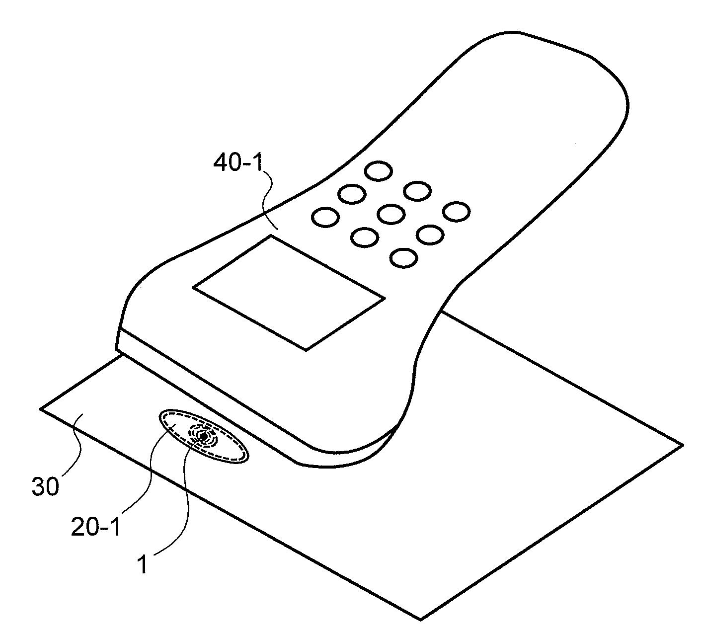
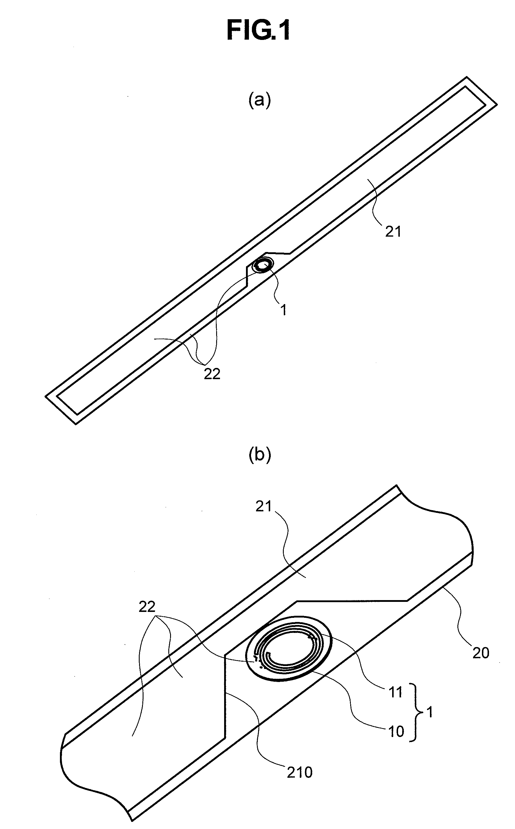
[0042]FIGS. 1A and 1B are typical external perspective views of an RF-ID circuit apparatus (or RFID tag) to which the invention is applied. FIG. 1A shows the entire RF-ID circuit apparatus, and FIG. 1B is a detail diagram of the surrounding of a circuit chip (such as an IC chip) 1. The circuit chip 1 has a whorl antenna coil 11 on a circuit surface of a disk-shaped silicon chip 10, which is a circuit substrate. The circuit chip 1 uses the antenna coil 11 to receive radio waves and power from the outside and return signal radio waves to the outside for communication with the outside (such as a reader, writer and the composite circuit, not shown). The antenna coil 11 implementing the information exchange between the circuit chip 1 and the external circuit may be coated with gold plating, for example, as an upper wire on the circuit surface side of the silicon chip 10 (that is, the base material of the circuit chip 1). A base film 20 having an antenna 21 of aluminum foil, for example, ...

second embodiment

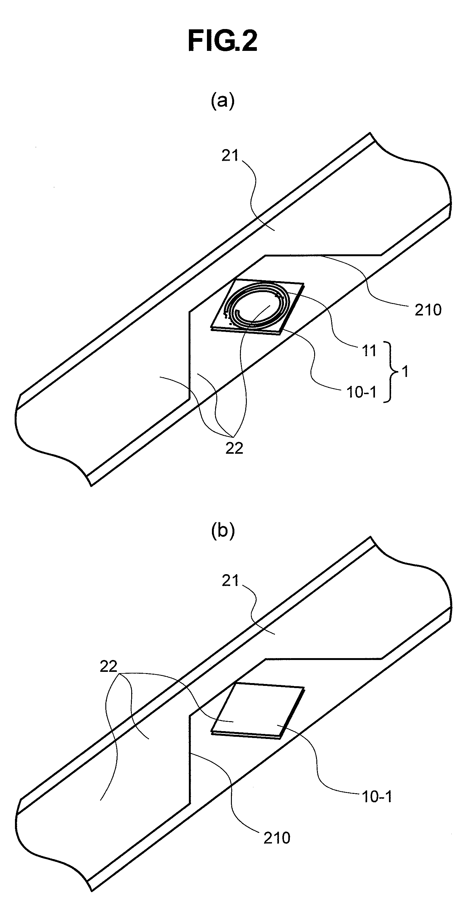
[0050]FIGS. 2A and 2B show a similar antenna structure to that of the first embodiment described with reference to FIGS. 1A and 1B except that the circuit chip 1 includes a square-shaped circuit substrate 10-1. According to this embodiment, the antenna coil 11 and the antenna 21 are only placed closely, but connection by the mutual contact is not required. Therefore, the limitations on the mounting position, angle and front or back of the circuit chip 1 on the main surface of the base film 20 can be alleviated. For example, as shown in FIG. 2B, even when the circuit substrate 10-1 is mounted on the main surface of the base film 20 upside down, no problems occur like the first embodiment. Since the circuit chip 1 can be cut out by cutting a semiconductor base material such as a silicon wafer straight with a dicing blade for use in a general semiconductor post-process, the square-shaped circuit substrate 10-1 (or the circuit chip 1) can be obtained at low costs and from one silicon wa...

third embodiment

[0051]The RFID tag according to this embodiment, which will be described with reference to FIGS. 3A and 3B, is characterized by an antenna 21-1 which is formed in a straight line on the main surface of the base film 20. The dipole antenna 21-1 does not have a so-called notch at the center (or near the longitudinal middle point), unlike the antenna 21 according to the first and second embodiment. Also in this embodiment, the circuit chip 1 is only required to place near the center of the antenna 21-1, and the precision for aligning the chip can be more alleviated than that in the antenna 21 case. However, the communication condition between the circuit chip 1 and the antenna 21-1 depends on the attitude of an antenna coil 11 of the circuit chip 1 about a magnetic field H, which is induced by current i occurring in the dipole antenna 21-1, as shown in FIG. 3B. For example, when the circuit chip 1 is fixed to the main surface of the base film 20 at one side (or side wall), the strength...


PUM


Abstract

A circuit chip having a loop-shaped antenna coil on a main surface and a tag sheet having an antenna pattern on a main surface are prepared, and the circuit chip is mounted on the main surface of the tag sheet so as not to place over the antenna pattern. The circuit chip is placed closely to the antenna pattern, and at least the half of the main surface is desirably faced against the antenna pattern. Thus, signals and / or power can be securely exchanged between the circuit chip (or antenna coil) and the antenna pattern. Therefore, a high-performance and rigid RFID tag can be obtained by roughly aligning the circuit chip and the tag sheet.

Description

[0001]The present application claims priority from Japanese application JP 2007-241732 filed on Sep. 19, 2007, the content of which is hereby incorporated by reference into this application.BACKGROUND OF THE INVENTION[0002]1. Field of the Invention[0003]The present invention relates to a structure of an RFID tag and a manufacturing process for an RFID tag.[0004]2. Description of the Related Art[0005]A conventional semiconductor apparatus has a structure in which multiple connection terminals on a surface of an IC chip are contact-fixed to and electrically connected to a connection part of an antenna sheet of an RFID tag, as disclosed in JP-A-8-88586, which requires precise alignment and fixing of the connection terminals of the IC chip and the connection part of the antenna sheet. For that reason, if the IC chip is finer, the connection terminals are necessarily finer and must be placed closely to each other, requiring high precision is required for the alignment. In order to implem...

Claims


Application Information

Patent Timeline
Patent Type & Authority Applications(United States)
IPC IPC(8): G08B13/14
CPCG06K19/07749G06K19/07H01Q7/00
Inventor OROKU, NORIYUKIKANDA, NAOYAKANDO, HIDEHIKOUESAKA, KOUICHI
Owner SES RFID SOLUTIONS
Why Eureka
Try Eureka