Semiconductor device and method of forming the same as well as data processing system including the semiconductor device

a semiconductor device and semiconductor technology, applied in the direction of semiconductor devices, basic electric elements, electrical appliances, etc., can solve the problems of difficult control of the threshold voltage of the transistor, difficult to realize or implement a semiconductor device that needs to operate at a lower voltage, and difficult to further shrink the transistor. to achieve the effect of high driving voltag

Active Publication Date: 2009-04-02
NVIDIA CORP
View PDF3 Cites 56 Cited by
  • Summary
  • Abstract
  • Description
  • Claims
  • Application Information

AI Technical Summary

Benefits of technology

[0007]In one embodiment, a semiconductor device may include, but is not limited to, a substrate, a low voltage transistor over the substrate, and a high voltage transistor over the substrate. The low voltage transistor may be configured by at least one unit transistor. The high voltage transistor may be high in driving voltage than the low voltage transistor. The high voltage transistor may be configured by a greater number of the unit transistors than the at least one unit transistor that configures the low voltage transistor. Each of the unit transistors may include, but is not limited to, a vertically extending portion of semiconductor over the substrate, a gate insulating film extending along a side surface of the vertically extending port

Problems solved by technology

Further shrinkage of a transistor is difficult.
Shrinkage of a transistor may needs for further reduction in the gate length L of the transistor, thereby causing remarkable shot channel effects, and making it difficult to control the threshold voltage of the transistor.
Increase of the threshold voltage of the transistor due to the increase of S-value makes it difficult to realize or implement a semiconductor device that needs to operate at lower v

Method used


Image

  • Semiconductor device and method of forming the same as well as data processing system including the semiconductor device
  • Semiconductor device and method of forming the same as well as data processing system including the semiconductor device
  • Semiconductor device and method of forming the same as well as data processing system including the semiconductor device

Examples


first embodiment

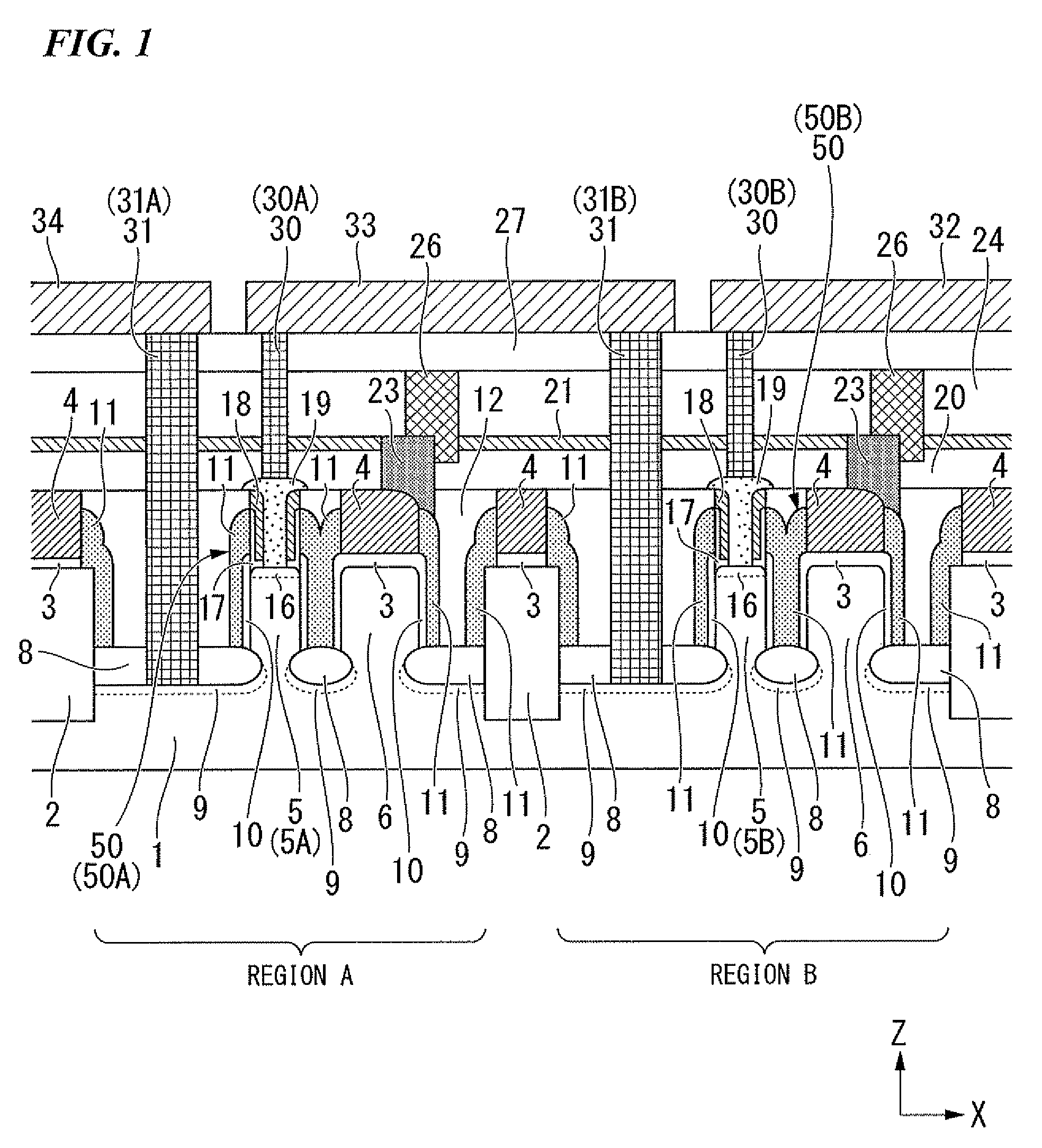
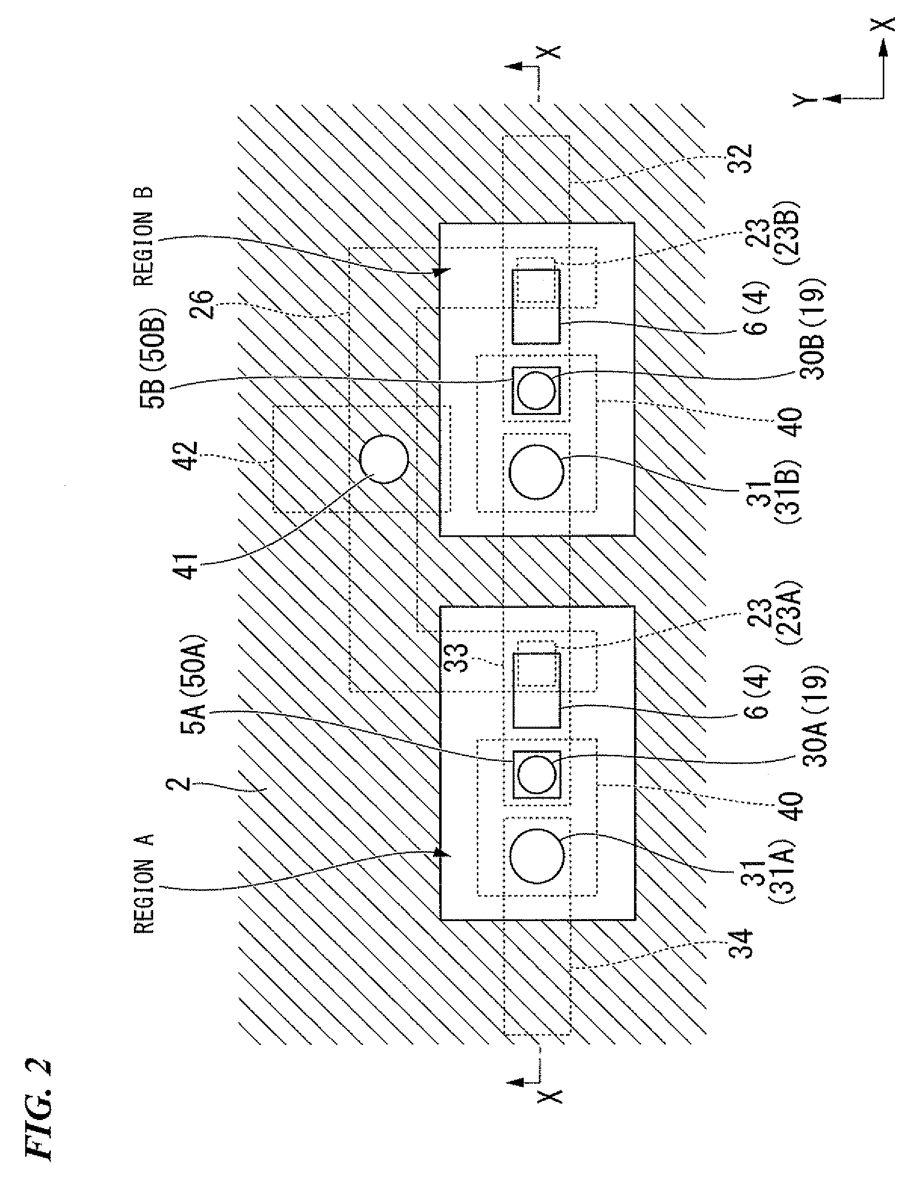
[0027]A semiconductor device will be described in accordance with a first preferred embodiment of the present invention. The semiconductor device includes an integration of high voltage transistors and low voltage transistors. The high voltage transistors are designed to operate with higher driving voltage than driving voltage for driving the low voltage transistors. FIG. 1 shows only the high voltage transistors but does not illustrate the low voltage transistors.

[0028]With reference to FIGS. 1 and 2, a shallow trench isolation 2 is selectively provided in an upper region of a silicon substrate 1. The shallow trench isolation 2 defines first and second active regions A and B. The first active region A includes a first unit transistor 50A. The first unit transistor 50A has a first silicon pillar 5A. The first silicon pillar 5A may be positioned at the center of the first active region A. The second active region B includes a second unit transistor 50B. The second unit transistor 50B...

second embodiment

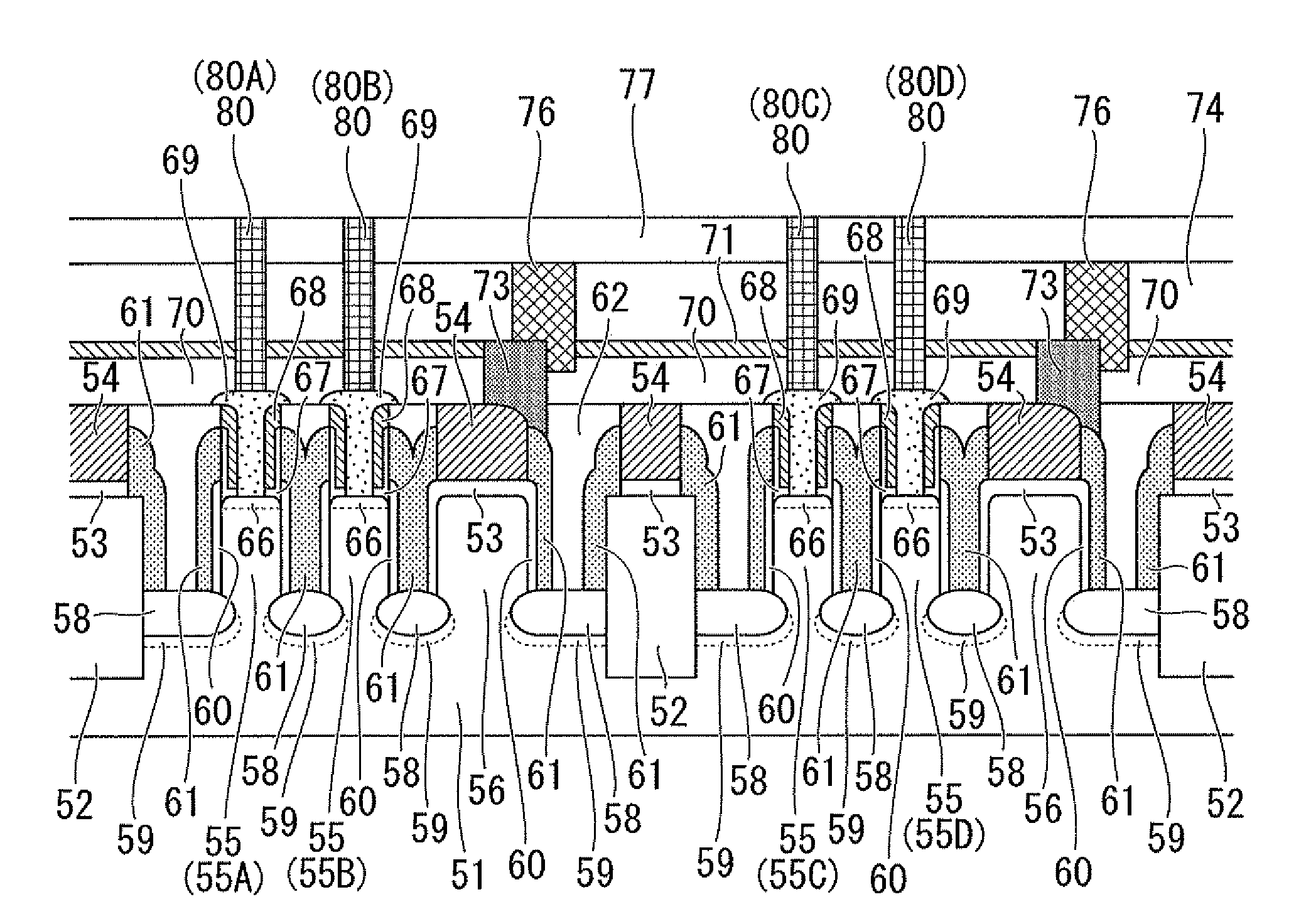
[0088]A semiconductor device will be described in accordance with a second preferred embodiment of the present invention. The semiconductor device includes an integration of high voltage transistors and low voltage transistors. The high voltage transistors are designed to operate with higher driving voltage than driving voltage for driving the low voltage transistors. FIG. 4 shows only the high voltage transistors but does not illustrate the low voltage transistors.

[0089]With reference to FIGS. 4 and 5, a shallow trench isolation 52 is selectively provided in an upper region of a silicon substrate 51. The shallow trench isolation 52 defines first and second active regions A and B. The first active region A includes first and second unit transistors 100A and 100B. The first unit transistor 100A has a first silicon pillar 55A. The second unit transistor 100B has a second silicon pillar 55B. The second silicon pillar 55B may be positioned at the center of the first active region A. The...


PUM


Abstract

A semiconductor device includes low voltage and high voltage transistors over a substrate. The low voltage transistor is configured by at least one unit transistor. The high voltage transistor is configured by a greater number of the unit transistors than the at least one unit transistor that configures the low voltage transistor. Each of the unit transistors may include a vertically extending portion of semiconductor providing a channel region and having a uniform height, a gate insulating film extending along a side surface of the vertically extending portion of semiconductor, a gate electrode separated by the gate insulating film from the vertically extending portion of semiconductor, and upper and lower diffusion regions being respectively disposed near the top and bottom of the vertically extending portion of semiconductor. The greater number of the unit transistors are connected in series to each other and have gate electrodes eclectically connected to each other.

Description

BACKGROUND OF THE INVENTION[0001]1. Field of the Invention[0002]The present invention generally relates to a semiconductor device and a method of forming the same. More specifically, the present invention relates to a semiconductor device including a vertical surround gate transistor structure and a method of forming the same as well as a data processing system including the semiconductor device.[0003]Priority is claimed on Japanese Patent Application No. 2007-254172, filed Sep. 28, 2007, the content of which is incorporated herein by reference.[0004]2. Description of the Related Art[0005]In recent years, there has been progressed high density integration and high performance of a semiconductor device with shrinkage of transistors that are integrated therein. Further shrinkage of a transistor is difficult. Shrinkage of a transistor may needs for further reduction in the gate length L of the transistor, thereby causing remarkable shot channel effects, and making it difficult to contr...

Claims


Application Information

Patent Timeline
IPC IPC(8): H01L29/00
CPCH01L21/823487H01L27/10894H01L29/7827H01L29/0692H01L29/66666H01L29/0653H10B12/09
Inventor TAKAISHI, YOSHIHIRO
Owner NVIDIA CORP
Why Eureka
Try Eureka