Eureka AIR delivers breakthrough ideas for toughest innovation challenges, trusted by R&D personnel around the world.

Integrated-circuit package for proximity communication

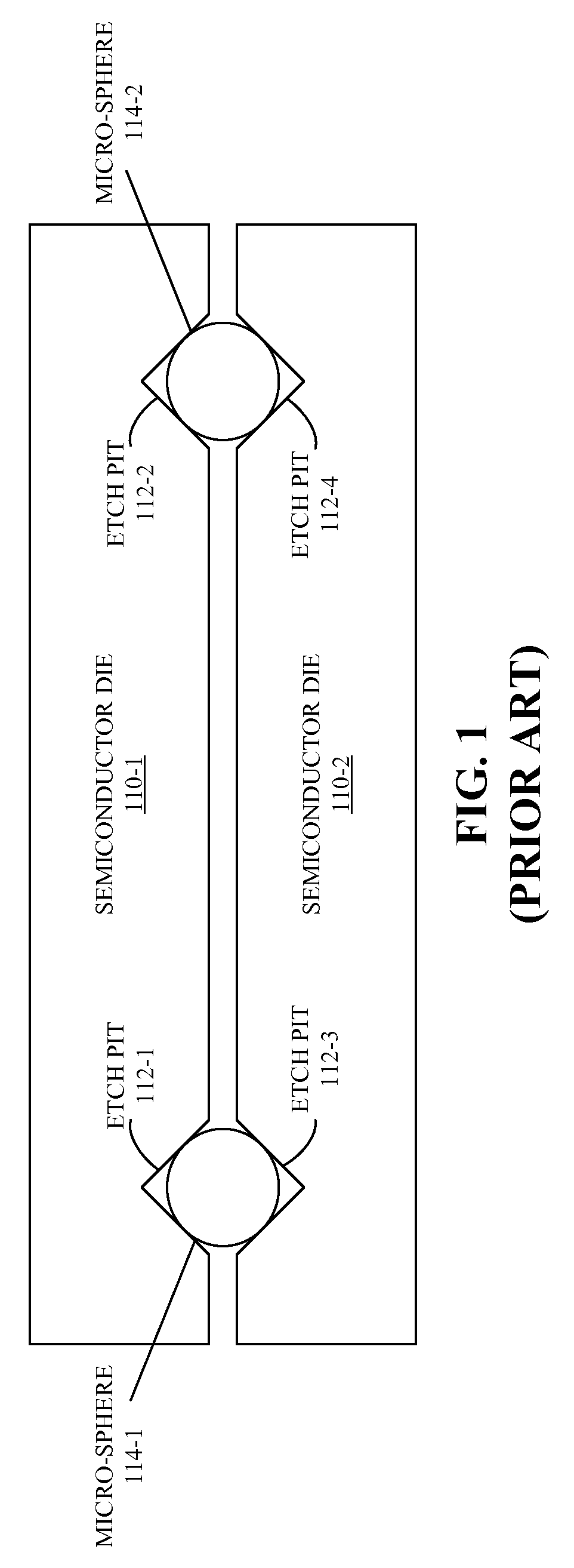
a technology of proximity communication and integrated circuit, which is applied in the direction of semiconductor devices, electrical equipment, semiconductor/solid-state device details, etc., can solve the problems of destroying received signals, bottlenecks that continue to grow, and inability to match the advances of inter-chip communication technology with the advancement of semiconductor technology, so as to facilitate the alignment of proximity connectors

Active Publication Date: 2009-04-02
ORACLE INT CORP
View PDF5 Cites 43 Cited by
  • Summary
  • Abstract
  • Description
  • Claims
  • Application Information

AI Technical Summary

Benefits of technology

[0015]One embodiment of the present invention provides a multi-chip module (MCM). This MCM includes a first semiconductor die and a second semiconductor die, where a given semiconductor die, which can be the first semiconductor die or the second semiconductor die, includes proximity connectors proximate to a surface of the given semiconductor die. Moreover, the given semiconductor die is configured to communicate signals with the other semiconductor die via proximity communication through one or more of the proximity connectors. Furthermore, the MCM includes an alignment plate and a top plate coupled to the alignment plate. This alignment plate includes a first negative feature configured to accommodate the first semiconductor die and a second negative feature configured to accommodate the second semiconductor die, and the top plate includes a positive feature. Note that the positive feature is coupled to the first semiconductor die, and the positive feature facilitates mechanical positioning of the first semiconductor die.
[0021]In some embodiments, the MCM includes a base plate coupled to the alignment plate, where the first semiconductor die is coupled to the base plate using second coupling elements which facilitate the mechanical positioning. These second coupling elements may include micro-spheres. In some embodiments, the micro-spheres are positioned into depressions in the base plate and depressions in the alignment plate. Moreover, the second coupling elements may facilitate an orientation of the first semiconductor die.
[0025]Another embodiments provides a method for assembling the MCM. During this process, a first semiconductor die is positioned into a first negative feature in the alignment plate in the MCM, where the positioning involves coupling the first semiconductor die to the base plate in the MCM using fourth coupling elements. Then, a second semiconductor die is positioned into a second negative feature in the alignment plate, where the positioning involves coupling the second semiconductor die to the base plate using fifth coupling elements. Next, the first semiconductor die is coupled to the second semiconductor die using third coupling elements. Note that given coupling elements, which can include the first coupling elements, the second coupling elements, or the third coupling elements, facilitate aligning of proximity connectors proximate to a first surface of the first semiconductor die with proximity connectors proximate to a second surface of the second semiconductor die.

Problems solved by technology

Unfortunately, these advances in semiconductor technology have not been matched by corresponding advances in inter-chip communication technology.
This problem has created a bottleneck that continues to grow as semiconductor integration densities continue to increase.
Misalignment between the transmitter pads and the receiver pads may cause each receiving pad to span two transmitting pads, thereby destroying a received signal.
Unfortunately, it can be very challenging to align chips properly.
Consequently, this approach may add complexity and cost to the process of assembling MCMs.
Moreover, proximity communication poses addition challenges in the design and assembly of MCMs, including: providing power to the chips; effectively cooling the chips; interfacing the MCMs to external input / output (I / O) mechanisms; testing; reliability in the presence of perturbations, such as thermal stress, vibration, and mechanical shock; and the ability to rework MCMs to repair and / or replace components that do not work.

Method used


Image

  • Integrated-circuit package for proximity communication
  • Integrated-circuit package for proximity communication
  • Integrated-circuit package for proximity communication

Examples


Embodiment Construction

[0046]The following description is presented to enable any person skilled in the art to make and use the invention, and is provided in the context of a particular application and its requirements. Various modifications to the disclosed embodiments will be readily apparent to those skilled in the art, and the general principles defined herein may be applied to other embodiments and applications without departing from the spirit and scope of the present invention. Thus, the present invention is not intended to be limited to the embodiments shown, but is to be accorded the widest scope consistent with the principles and features disclosed herein.

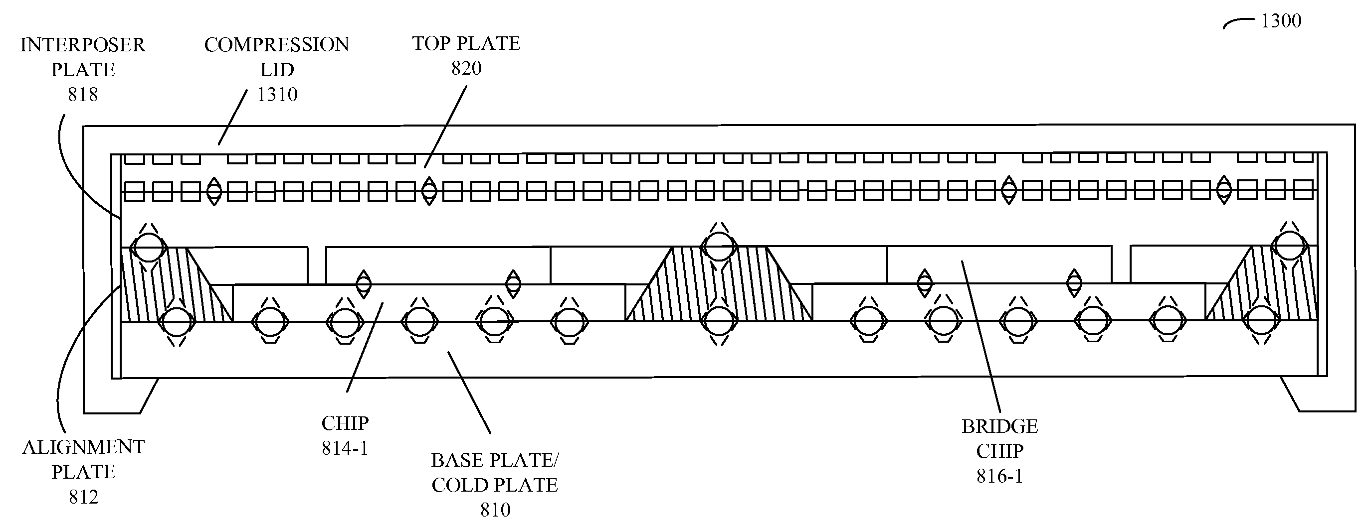
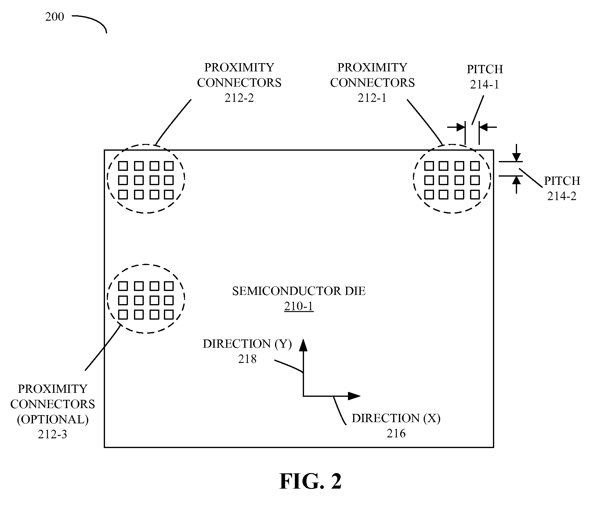
[0047]Embodiments of a method, a semiconductor die, an MCM, and systems that include the MCM are described. Note that the MCM, which is sometimes referred to as a macro-chip, includes an array of chip modules (CMs) or single-chip modules (SCMs), and a given SCM includes at least one semiconductor die. Furthermore, the semiconductor die communic...


PUM


Abstract

Embodiments of a multi-chip module (MCM) are described. This MCM includes a first semiconductor die and a second semiconductor die, where a given semiconductor die, which can be the first semiconductor die or the second semiconductor die, includes proximity connectors proximate to a surface of the given semiconductor die. Moreover, the given semiconductor die is configured to communicate signals with the other semiconductor die via proximity communication through one or more of the proximity connectors. Furthermore, the MCM includes an alignment plate and a top plate coupled to the alignment plate. This alignment plate includes a first negative feature configured to accommodate the first semiconductor die and a second negative feature configured to accommodate the second semiconductor die, and the top plate includes a positive feature. Note that the positive feature is coupled to the first semiconductor die, and the positive feature facilitates mechanical positioning of the first semiconductor die.

Description

CROSS REFERENCE TO RELATED APPLICATIONS[0001]This application is related to pending U.S. patent application Ser. No. 11 / 243,300, filed on Oct. 3, 2005, the contents of which are herein incorporated by reference.GOVERNMENT LICENSE RIGHTS[0002]This invention was made with United States Government support under Contract No. NBCH3039002 awarded by the Defense Advanced Research Projects Administration. The United States Government has certain rights in the invention.BACKGROUND[0003]1. Field of the Invention[0004]The present invention relates to techniques for packaging integrated circuits. More specifically, the present invention relates to a multi-chip module that facilitates inter-chip proximity communication.[0005]2. Related Art[0006]Advances in semiconductor technology presently make it possible to integrate large-scale systems, which can include hundreds of millions of transistors, into a single semiconductor chip (or die). Integrating such large-scale systems onto a single semicond...

Claims


Application Information

Patent Timeline
IPC IPC(8): H01L23/02H01L21/00
CPCH01L23/10H01L23/48H01L2924/10253H01L24/02H01L24/16H01L24/72H01L24/81H01L24/95H01L25/0652H01L25/50H01L2224/0401H01L2224/13099H01L2224/81136H01L2224/81801H01L2224/95136H01L2225/06513H01L2225/06593H01L2924/01004H01L2924/01013H01L2924/01014H01L2924/01029H01L2924/01058H01L2924/01074H01L2924/01079H01L2924/01082H01L2924/014H01L2924/10157H01L2924/10158H01L2924/14H01L2924/1433H01L2924/01006H01L2924/01019H01L2924/01023H01L2924/01033H01L2924/01067H01L2924/01076H01L2225/06534H01L2225/06531H01L2924/00H01L2924/351H01L2224/73251H01L2224/16H01L2224/72
Inventor MITCHELL, JAMES G.CUNNINGHAM, JOHN E.KRISHNAMOORTHY, ASHOK V.
Owner ORACLE INT CORP
Why Eureka
Eureka Blog
Learn More