Method for manufacturing an electronic component package and electronic component package

a technology of electronic components and components, applied in the direction of electrical equipment, semiconductor devices, semiconductor/solid-state device details, etc., can solve the problems of inability to carry out photolithography under good conditions, inability to form uniform layers, and inability to uniformly develop through resist layers

Inactive Publication Date: 2009-04-02
KK TOSHIBA
View PDF7 Cites 131 Cited by
  • Summary
  • Abstract
  • Description
  • Claims
  • Application Information

AI Technical Summary

Problems solved by technology

In this point of view, if some convex-concave portions are formed on the semiconductor wafer, the resist layer can not formed uniformly so that the developing can not be carried out uniformly through the resist layer.
As a result, the photolithography can not be carried out under good condition and thus, the intended electronic component packages can not be obtained.

Method used


Image

  • Method for manufacturing an electronic component package and electronic component package
  • Method for manufacturing an electronic component package and electronic component package
  • Method for manufacturing an electronic component package and electronic component package

Examples


first embodiment

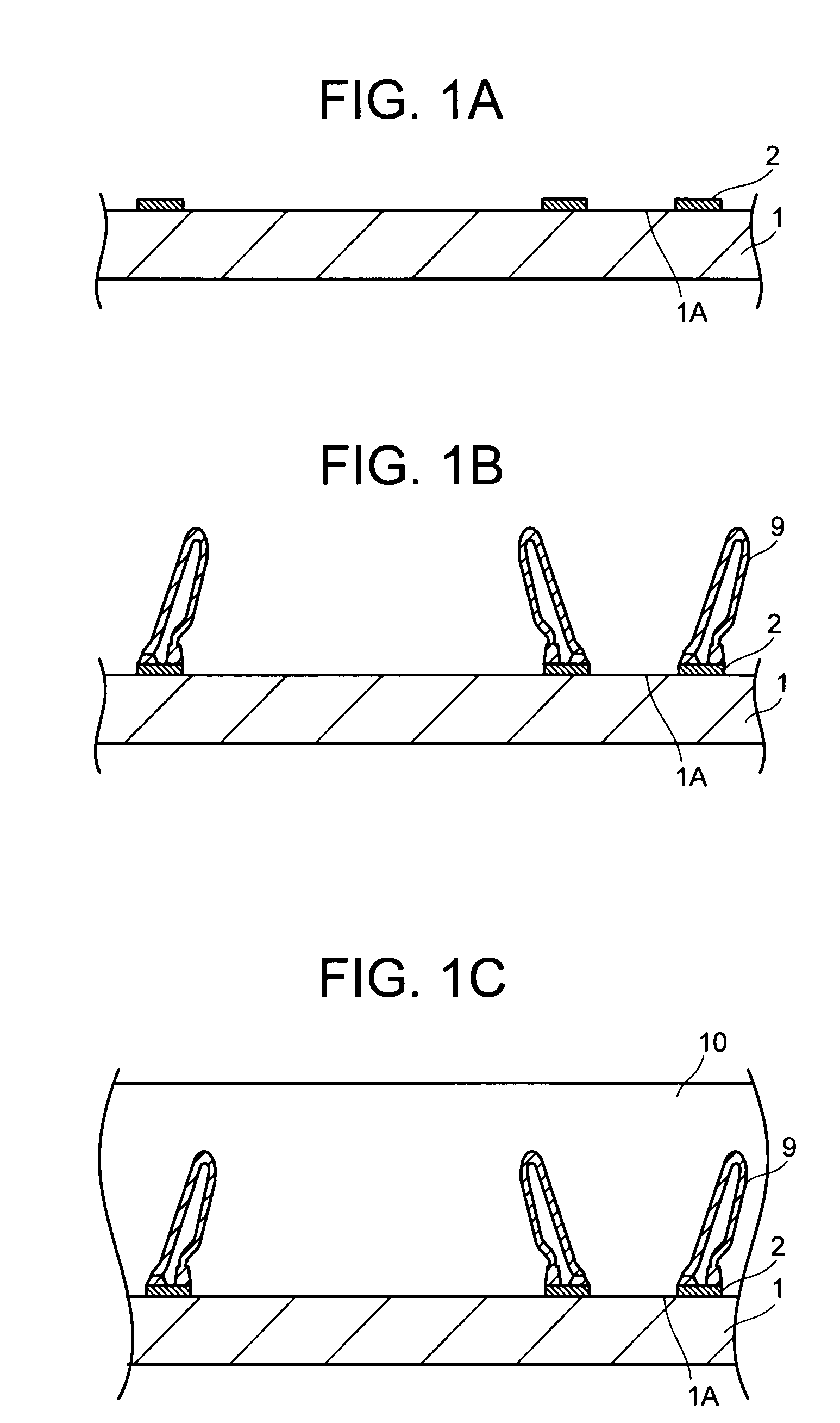
[0017]FIGS. 1 and 2 relate to steps in a method for manufacturing an electronic component package according to a first embodiment.

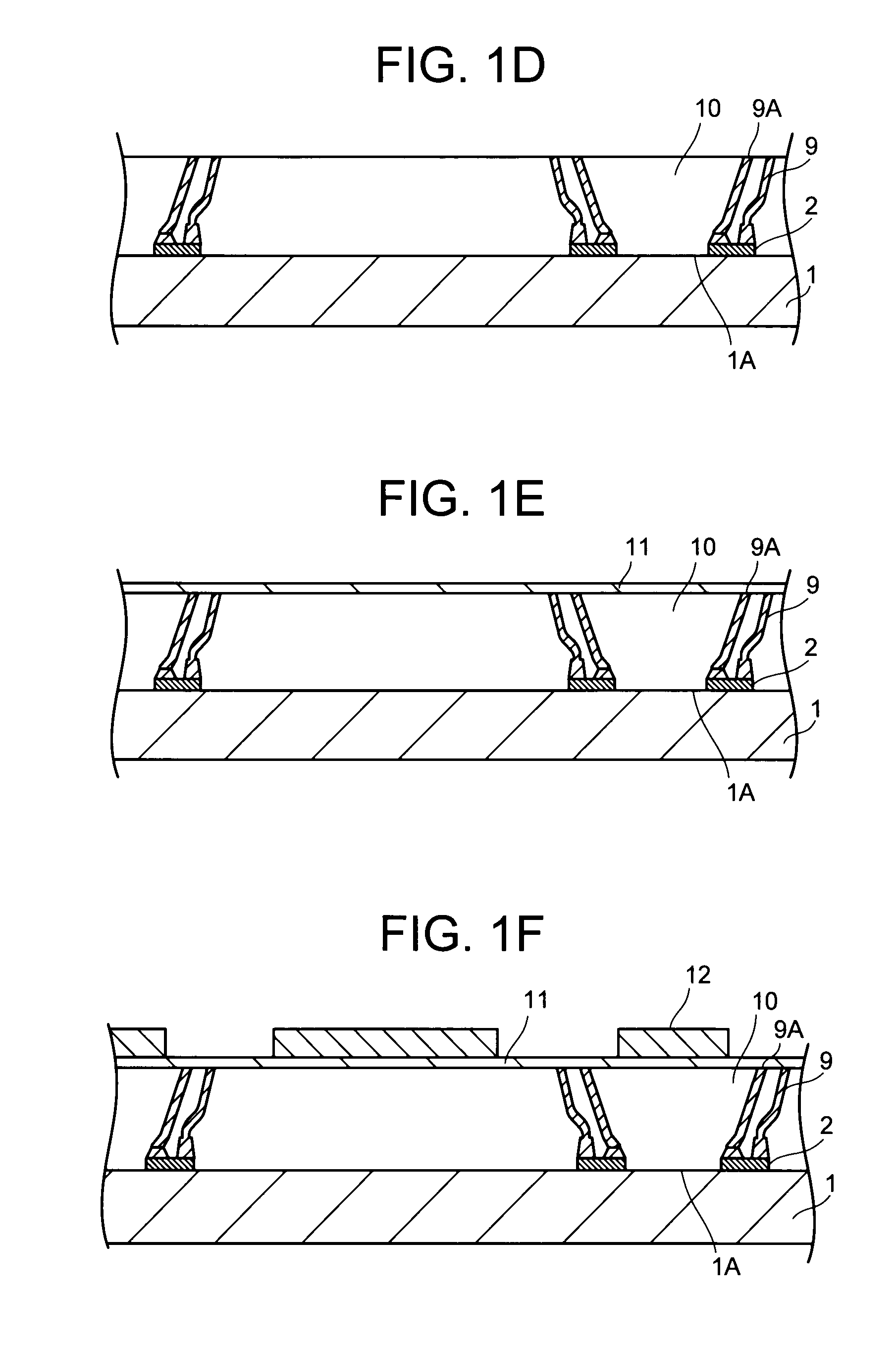
[0018]As shown in FIG. 1A, electrode pads 2 are formed on a main surface 1A of a semiconductor wafer (electronic component) 1, e.g., with integrated circuits thereon. As shown in FIG. 1B, then, bonding wires 9 are formed on the electrode pads 2, respectively so as to be elongated upward and shaped in loop. As shown in FIG. 1C, then, a surface protective resin layer 10 is applied thick on the main surface 1A of the semiconductor wafer 1 so as to embed the bonding wires 9.

[0019]The resin layer 10 may be formed by screen printing, dispensing, splay coating, spin coating. Preferably, the resin layer 10 is formed by screen printing because a low expansion resin containing inorganic fillers can be applied effectively according to the screen printing. With the screen printing, the periphery of the semiconductor wafer is not partially coated because the edge of t...

second embodiment

[0027]FIG. 3 relates to steps in a method for manufacturing an electronic component package according to a second embodiment.

[0028]As shown in FIG. 3A, the patterned electrode pads 2 are formed on the main surface 1A of the semiconductor wafer (electronic component) 1. As shown in FIG. 3B, then, the bonding wires 9 are formed so as to be bridged between the adjacent electrode pads 2, elongated upward and shaped in trapezoid, respectively. As shown in FIG. 3C, then, the surface protective resin layer 10 is applied thick on the main surface 1A of the semiconductor wafer 1 so as to embed the bonding wires 9.

[0029]Then, after the surface protective resin layer 10 is hardened, as shown in FIG. 3D, the resin layer 10 is polished at the surface level lower than the upper bases of the bonding wires 9 so as to expose the ends 9A of the bonding wires 9.

[0030]Then, as shown in FIG. 3E, the barrier metal 11 is formed over the grinded surface protective resin layer 10 and a resist layer is forme...

third embodiment

[0032]In this embodiment, the configuration of a wire bonder for forming the looped bonding wire will be described. FIG. 4 relates to the process flow about the use of the wire bonder. The wire bonder shown in FIG. 4 includes an ultrasonic transducer 15, a conical tube 14 (called as a “capillary”) made of ruby and provided at the end of the ultrasonic transducer 15, a bonding wire 9 provided through the capillary 14, a clamper 16 for pinching and fixing the bonding wire 9 which is disposed above the capillary 14 and a torch (not shown) for melting the forefront of the bonding wire through the electric discharge for the bonding wire to form a ball 9C. The torch is disposed in the vicinity of the capillary 14.

[0033]After the ball 9C is formed at the forefront of the bonding wire 9 by the torch (FIG. 4A), the ball 9C is fixed on the electrode pad 2 by ultrasonic connection. On the electrode pad 2 is formed the one end of the bonding wire 9 shaped in loop as described above (FIG. 4B). T...


PUM


Abstract

A manufacturing method of an electronic component package, includes: forming electrode pads on a main surface of a first electronic component; forming first bonding wires shaped in loop so as to be electrically connected with the electrode pads and elongated upward from the electrode pads and such that both ends of the first bonding wires are on the electrode pad, respectively; forming a resin layer over the main surface of the first electronic component so as to embed the first bonding wires; removing the resin layer so as to expose ends of the first bonding wires from the resin layer and removing the end of each of the first bonding wires so that two wires are elongated from on each of the electrode pads; and forming a metallic layer on the surface of the resin layer after removing so that the first bonding wires are electrically connected with the metallic layer.

Description

CROSS-REFERENCE TO RELATED APPLICATIONS[0001]This application is based upon and claims the benefit of priority from the prior Japanese Patent Application No. 2007-256189 filed on Sep. 28, 2007; the entire contents which are incorporated herein by reference.BACKGROUND OF THE INVENTION[0002]Conventionally, wafer level packaging technique such as Chip Scale Package (hereinafter, called as “CSP”) has been proposed. In the wafer level packaging technique, a resin for protecting the surface of each semiconductor chip is applied on a semiconductor wafer and the electrode pads for each semiconductor chip are also provided on the semiconductor wafer so as to form a semiconductor wafer assembly. Then, the semiconductor wafer assembly is divided into semiconductor electronic component packages. Concretely, a first insulating film is formed on a semiconductor wafer with electrode pads thereon so that the electrode pads can be exposed. Then, a redistribution layer is formed and a second insulati...

Claims


Application Information

Patent Timeline
Patent Type & Authority Applications(United States)
IPC IPC(8): H01L21/768H01L23/488
CPCB81B7/007H01L2224/02319H01L21/561H01L23/3114H01L24/18H01L24/82H01L2224/18H01L2224/73204H01L2224/73265H01L2924/01029H01L2924/01046H01L2924/01078H01L2924/01079H01L2924/14H01L2924/15311H01L2924/30105H01L2924/30107H01L2924/01005H01L2924/01006H01L2924/01019H01L2924/01033H01L2224/16225H01L2224/32225B81B2207/098H01L23/49811H01L2224/04042H01L2924/1461H01L2224/16145H01L2224/32145H01L2224/48145H01L2224/0401H01L2225/06568H01L2225/06506H01L2224/04105H01L2924/00H01L2924/00012H01L24/19H01L24/73H01L2224/12105H01L2924/3511
Inventor SUGIZAKI, YOSHIAKI
Owner KK TOSHIBA
Why Eureka
Try Eureka