Compensation of field effect on polycrystalline resistors

a polycrystalline resistor and field effect technology, applied in the field of electric circuitry, can solve the problems of metallization layer, inefficient use of bootstrapped resistors in die area (and therefore cost), and difficulty in overlaying each polycrystalline resistor

Active Publication Date: 2009-04-02
CIRRUS LOGIC INC
View PDF3 Cites 10 Cited by
  • Summary
  • Abstract
  • Description
  • Claims
  • Application Information

AI Technical Summary

Benefits of technology

[0009]The present invention provides improved apparatus, systems and methods. According to one embodiment, a resistive circuit includes a first terminal and a second terminal and polycrystalline first and second resistive segments coupled between the first and second terminals. A third terminal A is coupled to the first resistive segment, and a third terminal B is coupled to the second resistive segment. The third terminal A has a first voltage with respect to the first terminal, and the third terminal B has a second voltage with respect to the second terminal. With this arrangement, the non-linearity of resistance of the first resistive segment at least partially compensates for non-linearity of resistance of the second resistive segment.

Problems solved by technology

In addition, circuit layout considerations often make it difficult to overlay each polycrystalline resistor 106 with a metallization layer 110.
Although the bootstrapped resistor design employed in the embodiment of FIG. 1B can be effective in avoiding non-linear variations in resistivity to a first order approximation, both the well width W and well-to-well distance D are typically large, meaning that the use of bootstrapped resistors is inefficient in terms of die area (and therefore cost).

Method used


Image

  • Compensation of field effect on polycrystalline resistors
  • Compensation of field effect on polycrystalline resistors
  • Compensation of field effect on polycrystalline resistors

Examples


first embodiment

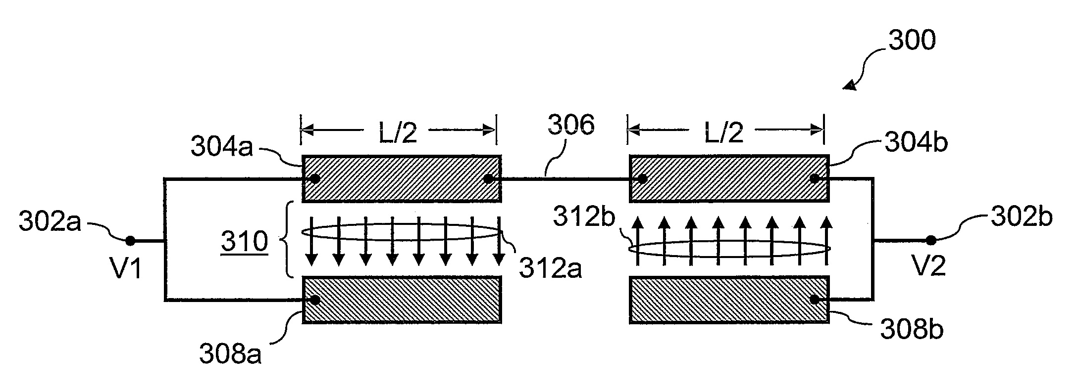
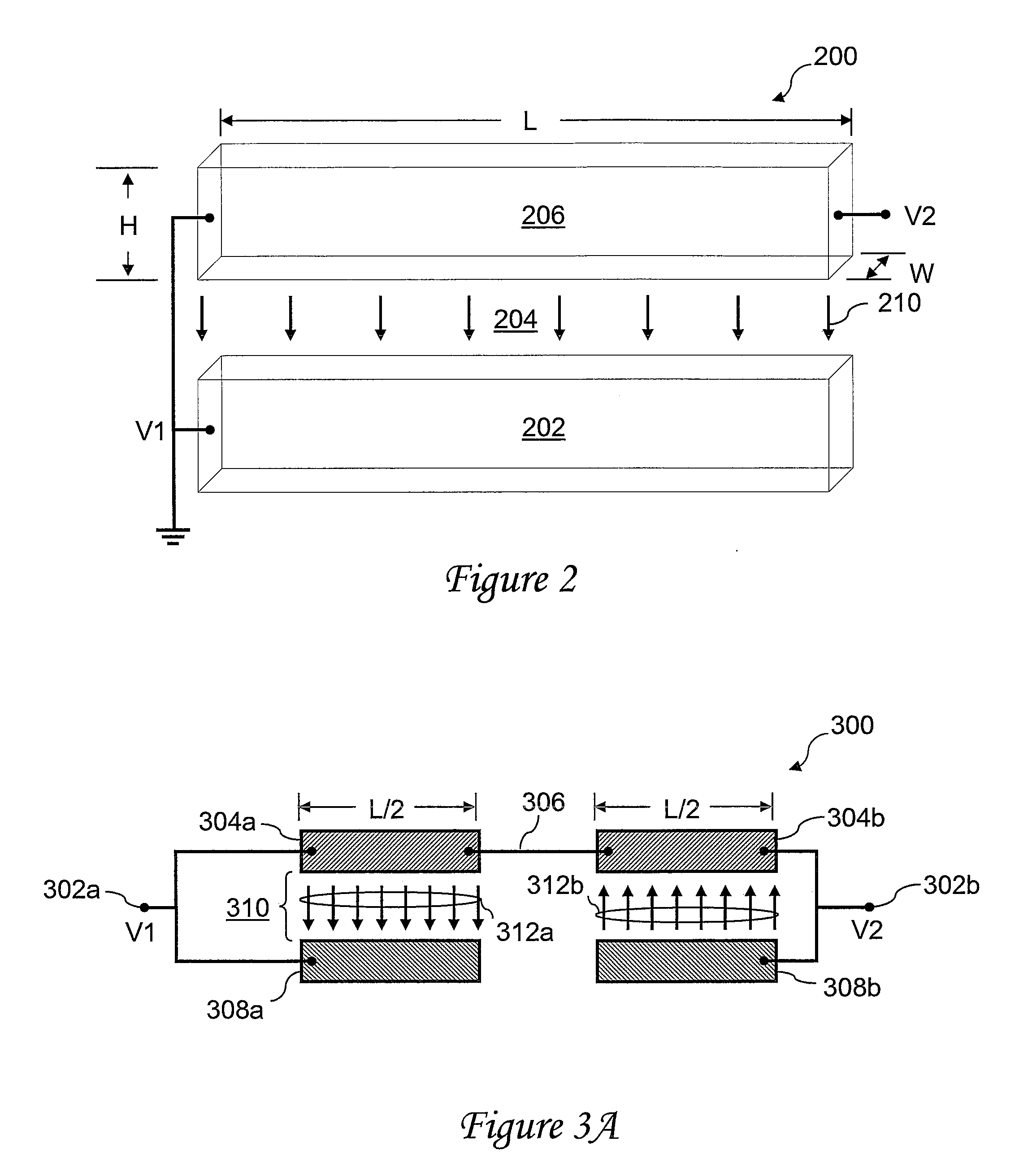
[0035]Referring now to FIG. 3A, there is illustrated a section view of a resistive circuit 300 in accordance with the present invention. As depicted, resistive circuit 300 includes a first terminal 302a characterized by voltage V1 and a second terminal 302b characterized by voltage V2, where voltage V2>voltage V1. Coupled between terminals 302a, 302b are multiple (in this case, two) resistive segments 304a, 304b formed of polycrystalline silicon or other resistive material subject to non-linear behavior when subjected to an electric field. Resistive segments 304 are spaced apart from one another and electrically coupled to each other, in this case in series, by a conductor 306, such as a metal.

[0036]Resistive circuit 300 further includes multiple third terminals 308a, 308b equal in number to the number of resistive segments 304. Each third terminal 308 is coupled at one end to an end of a respective resistive segment 304, in this case at one of first and second terminals 302a, 302b....

second embodiment

[0039]FIG. 3B depicts a resistive circuit 314 in accordance with the present invention. The embodiment of FIG. 3B is identical to that of FIG. 3A, except that the embodiment of FIG. 3B includes multiple third terminals for each resistive segment 304. That is, third terminals 308a1 and 308a2 apply positive electric fields 312a1 and 312a2 to resistive segment 304a, and third terminals 308b1 and 308b2 apply negative electric fields 312b1 and 312b2 to resistive segment 304b. It will be appreciated that not all third terminals for a resistive circuit are required to be formed of the same material. For example, in some implementations, third terminals 308a1 and 308b1 are implemented as substrate wells, and some third terminals 308a2 and 308b2 are implemented with metallizations.

third embodiment

[0040]FIG. 3C illustrates a resistive circuit 316 in accordance with the present invention. The embodiment of FIG. 3C is similar to that of FIG. 3A, except that third terminals 308a, 308b are directly connected to one another and are each electrically connected to the ends of resistive segments 304a, 304b distal from terminal 302a, 302b. As a result of this connection, third terminal 308a applies a negative electric field to resistive segment 304a, and third terminal 308b applies a positive electric field to resistive segment 304b.

[0041]FIG. 3D illustrates a fourth embodiment of a resistive circuit 320 in accordance with the present invention. The fourth embodiment of FIG. 3D employs a central connection of the segmented third terminal to the resistive segments similarly to the embodiment of FIG. 3C, but includes multiple third terminals for each resistive segment 304 as described above with reference to FIG. 3B. As depicted, third terminals 308a1 and 308a2 apply negative electric ...


PUM


Abstract

A resistive circuit includes a first terminal and a second terminal and polycrystalline first and second resistive segments coupled between the first and second terminals. A third terminal A is coupled to the first resistive segment, and a third terminal B is coupled to the second resistive segment. The third terminal A has a first voltage with respect to the first terminal, and the third terminal B has a second voltage with respect to the second terminal. With this arrangement, the non-linearity of resistance of the first resistive segment at least partially compensates for non-linearity of resistance of the second resistive segment.

Description

BACKGROUND OF THE INVENTION[0001]1. Technical Field[0002]The present invention relates in general to electrical circuitry, and more particularly, to the compensation of field effect on polycrystalline resistors.[0003]2. Description of the Related Art[0004]It is well known in the art of analog integrated circuitry that the resistance of polycrystalline silicon (also referred to as polysilicon, poly-Si or simply poly) varies with the applied voltage in a non-linear fashion in the presence of an electric field. This non-linearity is caused by an accumulation of carriers (and thus reduced resistance) in the presence of a positive electric field, or conversely, by a depletion of carriers (and thus increased resistance) in the presence of a negative electric field. Additional information regarding the non-linearity of polycrystalline silicon resistors can be found, for example, in Sze, S. M., Physics of Semiconductor Devices, 2nd Ed., pp. 362-366.[0005]Because such non-linearity is undesi...

Claims


Application Information

Patent Timeline
Patent Type & Authority Applications(United States)
IPC IPC(8): H03F1/36H01L29/00
CPCH03F1/32H03F2203/45528H03F2203/45136H03F3/45475H03F1/3211
Inventor YANG, HUAPRASAD, AMMISETTIMELANSON, JOHN L.
Owner CIRRUS LOGIC INC
Why Eureka
Try Eureka