Semiconductor package having semiconductor device featuring externally-accessible endless ring-shaped resistance circuit

a technology of resistance circuit and semiconductor device, which is applied in the direction of semiconductor device, semiconductor/solid-state device details, electrical apparatus, etc., can solve the problems of reducing the size of the package, affecting the performance of the package, and affecting the quality of the package, so as to achieve the effect of small siz

Inactive Publication Date: 2008-06-05
RENESAS ELECTRONICS CORP
View PDF6 Cites 16 Cited by
  • Summary
  • Abstract
  • Description
  • Claims
  • Application Information

AI Technical Summary

Benefits of technology

[0026]At least a part of the endless ring-like resistance circuit may be formed as a stacked conductive column. Preferably, the stacked conductive column includes via-structures and conductive layers alternately stacked.
[0027]The endless ring-shaped resistance circuit may include a plurality of lowermost conductive layers arranged along the periphery of the semiconductor device, a plurality of stacked conductive columns which are formed on ends of the lowermost conductive layers, and a plurality of uppermost conductive layers, each of which is formed on two stacked conductive columns formed on inner ends of two adjacent lowermost conductive layers.
[0028]Also, the endless ring-shaped resistance circuit may be defined as an endless seal-ring type resistance circuit including a plurality of endless ring-shaped conductive layers stacked in order.
[0029]The semiconductor device may further include a plurality of fourth electrode pads arranged beside the third electrode pads. Preferably, the fourth electrode pads have a smaller size than that of the third electrode pads.
[0030]The semiconductor device may further include a multi-layered insulating structure, and the endless ring-shaped resistance circuit is formed in the multi-layered insulating structure along a periphery thereof, with the third electrode pads being formed on a top surface of the multi-layered insulating structure.
[0031]The multi-layered insulating structure may include a plurality of insulating interlayers stacked in order, and at least a part of the endless ring-shaped resistance circuit is formed in each of the insulating interlayers. Each of the insulating interlayers may be composed of a low-k material, and the endless ring-shaped resistance circuit may be composed of copper (Cu).

Problems solved by technology

When the wire bonding process is carried out by the wire bonding machine, the low-k insulating interlayers of the multi-layered insulating structure are susceptible to a defect due to an impact which is produced when a bonding wire is bonded to each of the electrode pads on the semiconductor device.
On the other hand, when the moisture is absorbed by the low-k insulating interlayers of the multi-layered insulating structure, it takes a relatively long time until the absorbed moisture causes the corrosion in the conductive pattern layers formed in the interior of the multi-layered insulating structure.
Thus, a defect based on the corrosion may occur later in the conductive pattern layers.

Method used


Image

  • Semiconductor package having semiconductor device featuring externally-accessible endless ring-shaped resistance circuit
  • Semiconductor package having semiconductor device featuring externally-accessible endless ring-shaped resistance circuit
  • Semiconductor package having semiconductor device featuring externally-accessible endless ring-shaped resistance circuit

Examples


first embodiment

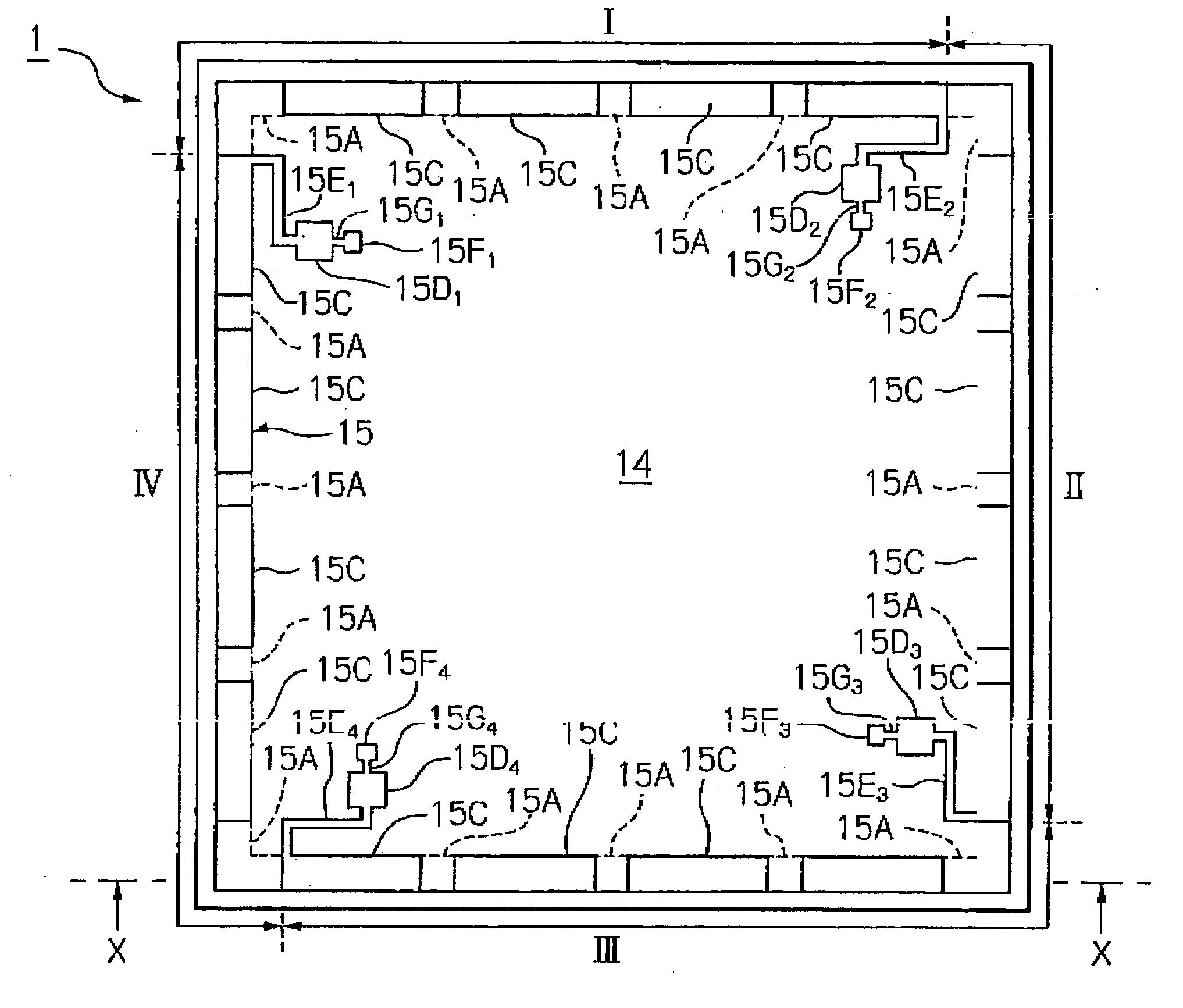
[0054]First, referring to FIGS. 3 and 4, a semiconductor device (chip), which is used in a first embodiment of the semiconductor package according to the present invention, is generally indicated by reference 1. Note that FIG. 3 is a plan view of the semiconductor device 1, and that FIG. 4 is a cross-sectional view taken along the X-X line of FIG. 3.

[0055]The semiconductor device 1 includes a rectangular semiconductor substrate such as a silicon substrate 12 (see: FIG. 4) derived from a monocrystalline silicon wafer, an insulating underlayer or contact layer 13 (see: FIG. 4) formed on a top surface of the silicon substrate 12, a multi-layered insulating structure 14 (see: FIGS. 3 and 4) formed on the contact layer 13, and an endless ring-shaped resistance circuit 15 (see: FIGS. 3 and 4) formed in the multi-layered insulating structure 14 along the sides of the silicon substrate 12.

[0056]Although not shown in FIG. 4, element-isolation layers are formed on the top surface of the silic...

second embodiment

[0103]With reference to FIG. 8 which is a cross-sectional view of a second embodiment of the semiconductor package according to the present invention, the second embodiment is substantially identical to the first embodiment of FIG. 7 except that an endless seal-ring type resistance circuit 15′ is substituted for the ring-shaped resistance circuit 15 having the meandering configuration (see: FIGS. 4, 5 and 6).

[0104]The endless seal-ring type resistance circuit 15′ includes a plurality of endless ring-shaped conductive layers 151 through 159 formed in the respective insulating interlayers 14, through 14, (see: FIG. 5) of the multi-layered insulating structure 14, with each of conductive layers 151, 152, 153 and 154 being defined as via-structures. The side walls of the multi-layered insulating structure 14 are covered with the endless seal-ring type resistance circuit 15′ so that moisture is prevented from being absorbed by the insulating interlayers 141 through 149.


PUM


Abstract

A semiconductor package includes a wiring board having a plurality of first electrode pads exposed on a top surface thereof, and a plurality of second electrode pads exposed on a bottom surface thereof, and the first electrode pads are electrically connected to the respective second electrode pads. A semiconductor device is mounted on the top surface of the wiring board, and includes an endless ring-shaped resistance circuit formed in an interior of the device along a periphery thereof, and a plurality of third electrode pads provided inside the resistance circuit and electrically connected to the resistance circuit. The third electrode pads are electrically connected to the first electrode pads, respectively. A sealing resin layer is formed over the first surface of the wiring board so that the device and the first electrode pads are sealed and protected by the sealing resin layer.

Description

BACKGROUND OF THE INVENTION[0001]1. Field of the Invention[0002]The present invention relates to a semiconductor package such as a ball grid array (BGA) type semiconductor package which includes a wiring board, a semiconductor device mounted on a top surface of the wiring board, a seating resin layer formed on the top surface of the wiring board so as to seal and protect the semiconductor device, and a plurality of external electrode terminals such as solder balls provided on a bottom surface of the wiring board.[0003]2. Description of the Related Art[0004]Conventionally, a semiconductor device used in a BGA type semiconductor package includes a rectangular-silicon substrate derived from a monocrystalline silicon wafer, an insulating underlayer or contact layer formed on a top surface of the silicon substrate, and a multi-layered-insulating structure formed on the contact layer.[0005]The multi-layered insulating structure includes a plurality of insulating interlayers stacked in ord...

Claims


Application Information

Patent Timeline
Patent Type & Authority Applications(United States)
IPC IPC(8): H01L23/485
CPCH01L23/3128H01L23/5228H01L23/585H01L2224/48091H01L2224/48227H01L2924/15311H01L2924/19041H01L2924/10253H01L2924/01019H01L24/48H01L2924/00014H01L2924/00H01L2924/181
Inventor UNO, SATOSHI
Owner RENESAS ELECTRONICS CORP
Why Eureka
Try Eureka