Method and system for improving wet chemical bath process stability and productivity in semiconductor manufacturing

Inactive Publication Date: 2009-04-02
TAIWAN SEMICON MFG CO LTD
View PDF4 Cites 12 Cited by
  • Summary
  • Abstract
  • Description
  • Claims
  • Application Information

AI Technical Summary

Benefits of technology

[0016]According to another aspect, a method for controlling process stability in a processing bath used for processing semiconductor substrates is provided. The method comprises providing a processing bath, performing a plurality of successive processing runs and, after each processing run, calculating Si concentration in the processing bath based on a film thickness parameter of a film that includes silicon and at least one further component. After performing the plurality of successive processing runs, the method provides for determining an aggregate Si concentration by adding each calculated Si concentration and an initial Si concentration value. The

Problems solved by technology

For example, as film thicknesses decrease and substrate sizes increase, it becomes increasingly challenging to completely and uniformly remove the thin film in a short time without attacking any underlying structures, i.e. so that the entire film clears at the same time.
One challenge in maintaining a constant etch or stripping rate, is that the etch or stripping rate is critically dependent on the concentration of the reactive chemical species in the bath, and this reactive chemical species is consumed during the etching/stripping operation.
This spiking procedure, however, is done infrequently and allows the chemical bath concentration to undesirably change run-to-run as it becomes depleted and also causes the chemical bath concentration to undesirably spike above desired concentration levels when the replenishing occurs.
Additionally, the reaction product between the reactive chemicals in the wet chemical bath and the material b

Method used


Image

  • Method and system for improving wet chemical bath process stability and productivity in semiconductor manufacturing
  • Method and system for improving wet chemical bath process stability and productivity in semiconductor manufacturing
  • Method and system for improving wet chemical bath process stability and productivity in semiconductor manufacturing

Examples


Example

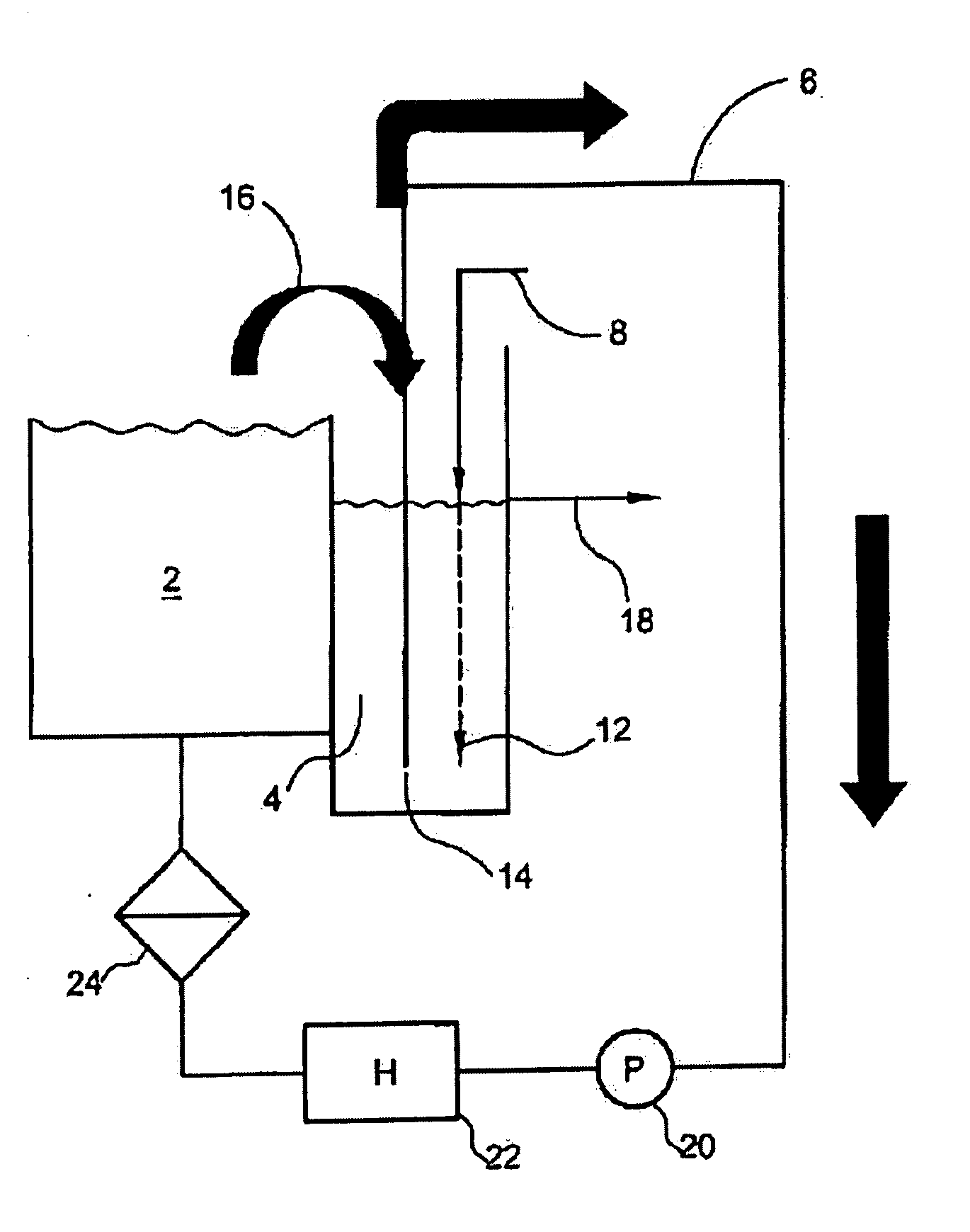
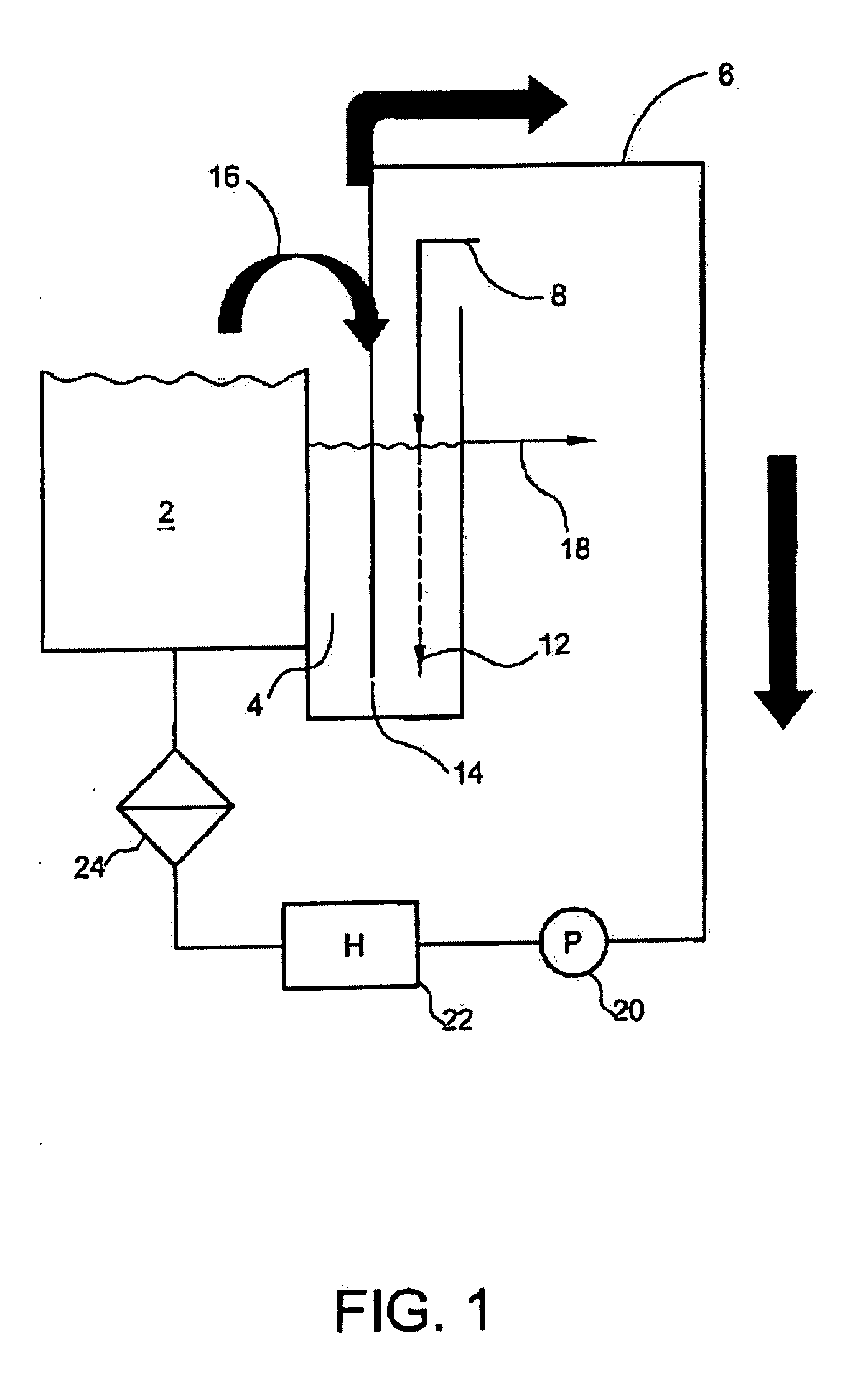
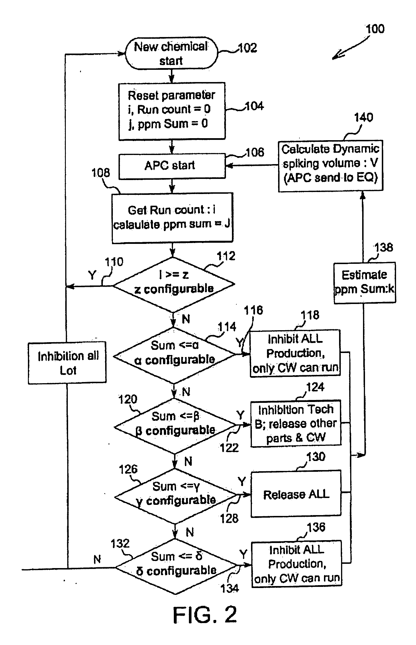
[0020]Provided is an automated process control (APC) method and system used in conjunction with a chemical or wet bath used in the manufacture of semiconductor devices. The method and system is applicable to various chemistries and although the following description will often be with respect to a hot phosphoric acid bath used to strip or etch a silicon nitride film, such is intended to be exemplary only and not limiting of the applications of the invention. According to other exemplary embodiments, the phosphoric acid bath may be used to strip or etch other silicon-containing films. According to other exemplary embodiments, a silicon nitride film may be etched or stripped by other chemicals and in still other exemplary embodiments, various other wet chemical baths may be used to etch or strip various other films, silicon-containing or otherwise, according to the concepts of the invention. A method and system for maintaining processing bath stability provides a processing bath in wh...


PUM

PropertyMeasurementUnit
Temperatureaaaaaaaaaa
Thicknessaaaaaaaaaa
Concentrationaaaaaaaaaa

Abstract

A chemical processing bath and system used in semiconductor manufacturing utilizes a dynamic spiking model that essentially constantly monitors chemical concentration in the processing bath and adds fresh chemical on a regular basis to maintain chemical concentrations at desirable levels. Etch rates and etch selectivities are maintained at desirable levels and contamination from undesirable precipitation is avoided. The system and method automatically compare concentration levels to a plurality of control limits associated with various technologies and identify the technology or technologies that may undergo processing.

Description

RELATED APPLICATION[0001]This application claims priority of U.S. Provisional Application Ser. No. 60 / 995,805, filed Sep. 28, 2007 and titled Universal APC Model to Improve Wet Bench Process Stability and Productivity, the contents of which are hereby incorporated by reference as if set forth in their entirety.FIELD OF THE INVENTION[0002]The present invention relates, most generally, to semiconductor device manufacturing. More particularly, the present invention relates to a method and system for stabilizing and controlling chemical solutions and processing systems used in etching, stripping, cleaning and other wet processing operations.BACKGROUND[0003]Semiconductor devices are formed on semiconductor substrates using a manufacturing process that typically includes several wet chemical processing operations. The wet processing operations include cleaning operations, stripping operations and etching operations in which the chemicals of the chemical bath react with a material such as ...

Claims


Application Information

Patent Timeline
IPC IPC(8): H01L21/66
CPCH01L21/67253H01L21/67086
Inventor YU, TAI-YUNGSU, YU-SHENGHSU, LI TELIANG, JIN LINYEH, SHIH CHENGSU, PIN CHIA
Owner TAIWAN SEMICON MFG CO LTD
Why Eureka
Try Eureka