Solar cells and methods and apparatuses for forming the same including i-layer and n-layer chamber cleaning

a technology of solar cells and chambers, applied in the direction of sustainable manufacturing/processing, final product manufacturing, coatings, etc., can solve the problems of high production costs of solar cells formed by these techniques, slow process, low device yield, etc., and achieve the effect of reducing contamination

Inactive Publication Date: 2009-04-09
APPLIED MATERIALS INC
View PDF100 Cites 248 Cited by
  • Summary
  • Abstract
  • Description
  • Claims
  • Application Information

AI Technical Summary

Benefits of technology

[0012]The present invention is directed to a method wherein there is provided a deposition system including a plurality of PECVD chambers wherein one chamber is dedicated to the deposition of a p-type amorphous silicon layer and the remainder of the chambers are each dedicated to the formation of an intrinsic silicon layer of amorphous or micro-crystalline structure or alternatively such an intrinsic layer (i-step) followed by an n-type layer (n-step). Subsequent to the deposition of the intrinsic and n-type layer, there is performed a passivation process step (pass-step) to reduce contamination. As an alternative embodiment of the present invention, a remote plasma cleaning process may be performed after a plurality of successive i-step / n-step / pass-step steps have been performed.

Problems solved by technology

Such a process is quite slow and requires an inordinate amount of time to complete thus creating high production costs for solar cells formed by these techniques.
Even when such deposition occurs, the throughput can be inadequate to obtain the desired production efficiencies and the achieved contamination levels can lead to a low device yield and generally poor device performance characteristics.

Method used


Image

  • Solar cells and methods and apparatuses for forming the same including i-layer and n-layer chamber cleaning
  • Solar cells and methods and apparatuses for forming the same including i-layer and n-layer chamber cleaning
  • Solar cells and methods and apparatuses for forming the same including i-layer and n-layer chamber cleaning

Examples


Embodiment Construction

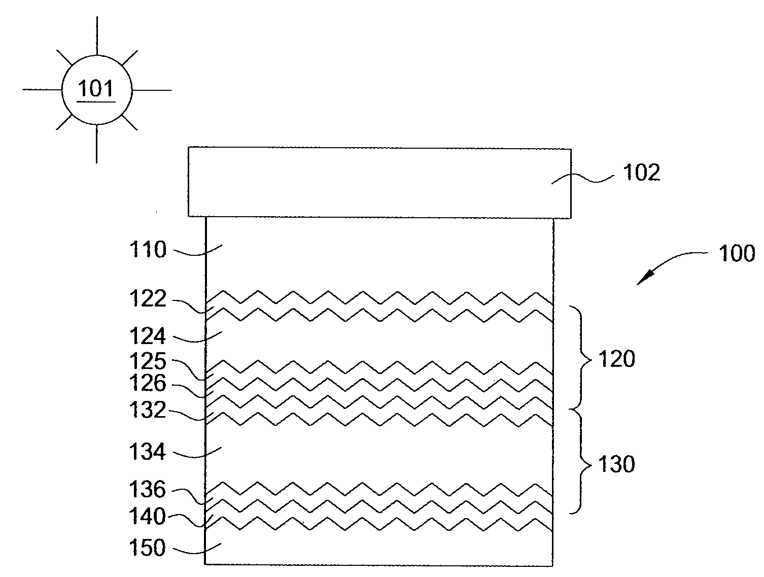
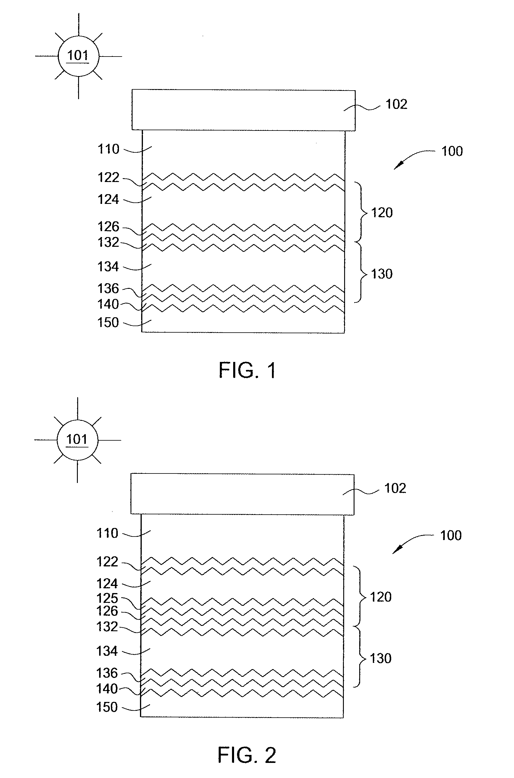
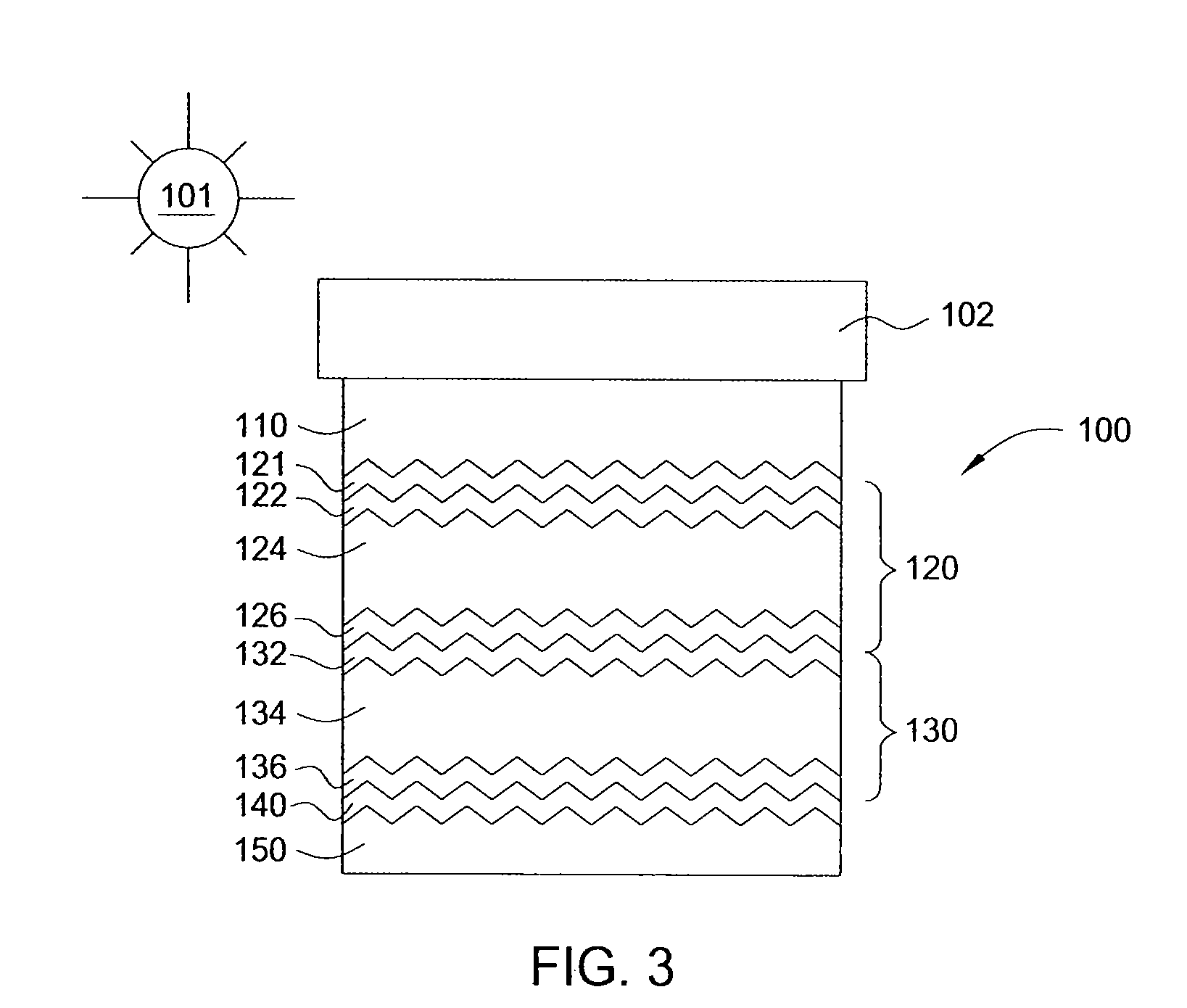
[0029]Embodiments of the present invention generally provide an apparatus and method for forming an improved thin film single-junction or multi-junction solar cell in a substrate processing device. One embodiment provides a system that contains at least one processing chamber that is adapted to deposit one or more layers that form a portion of a solar cell device. In one embodiment, a method is employed to reduce the contamination of a substrate processed in the processing chamber by performing a cleaning process on the inner surfaces of the processing chamber prior to depositing the one or more layers on a substrate. The cleaning process may include depositing a layer, such as a seasoning layer, that tends to trap contaminants found in the processing chamber, thus insuring that the processed substrate is clean, and future substrates processed in the chamber will have the same desirable process results. Other embodiments of the invention may provide scheduling and / or positioning the...


PUM

PropertyMeasurementUnit
frequencyaaaaaaaaaa
frequencyaaaaaaaaaa
frequencyaaaaaaaaaa

Abstract

Embodiments of the present invention generally provide an apparatus and method for forming an improved thin film single or multi-junction solar cell in a substrate processing device. One embodiment provides a system that contains at least one processing chamber that is adapted to deposit one or more layers that form a portion of a solar cell device. In one embodiment, a method is employed to reduce the contamination of a substrate processed in the processing chamber by performing a cleaning process on the inner surfaces of the processing chamber prior to depositing the one or more layers on a substrate. The cleaning process may include depositing a layer, such as a seasoning layer or passivation layer, that tends to trap contaminants found in the processing chamber. Other embodiments of the invention may provide scheduling and / or positioning the cleaning processing steps at desirable times within a substrate processing sequence to improve the overall system substrate throughput.

Description

CROSS-REFERENCE TO RELATED APPLICATIONS[0001]This application claims benefit of U.S. provisional patent application Ser. No. 60 / 958,904, filed Jul. 10, 2007, which is herein incorporated by reference.BACKGROUND OF THE INVENTION[0002]1. Field of the Invention[0003]The present invention generally relates to solar cells and methods and apparatuses for forming the same. More particularly, the present invention relates to thin film solar cells and methods and apparatuses for forming the same including steps used to control contamination and improve device yield.[0004]2. Description of the Related Art[0005]Plasma enhanced chemical vapor deposition (PECVD) chambers for the deposition of semiconductor materials on substrates is well known in the art. Examples of such PECVD chambers are shown in U.S. Pat. No. 6,477,980 and published Patent Application US 20060060138 each of which is incorporated herein by this reference. Plasma processes include supplying a process gas mixture to a vacuum ch...

Claims


Application Information

Patent Timeline
Patent Type & Authority Applications(United States)
IPC IPC(8): H01L21/02
CPCC23C16/24C23C16/4404C23C16/4408H01L21/67161H01L21/67745H01L31/076Y02E10/547H01L31/1824H01L31/1876H01L31/202Y02E10/545Y02E10/548Y10S438/906H01L31/1804Y02P70/50
Inventor CHOI, SOO YOUNGLI, LIWEI
Owner APPLIED MATERIALS INC
Why Eureka
Try Eureka