Wiring board and method of manufacturing the same

a wiring board and manufacturing method technology, applied in the field of wiring boards, can solve the problems of wiring board b>100/b> being easily deformed, and still generating deformation over the wiring board, so as to achieve the effect of reliably preventing a substrate deformation

Active Publication Date: 2009-04-16
SHINKO ELECTRIC IND CO LTD
View PDF3 Cites 20 Cited by
  • Summary
  • Abstract
  • Description
  • Claims
  • Application Information

AI Technical Summary

Benefits of technology

[0010]Exemplary embodiments of the present invention provide a wiring board which uses a resin as a reinforcing member and can reliably prevent a deformation of a substrate and a method of manufacturing the wiring board.

Problems solved by technology

However, the wiring board itself has a small mechanical strength.
Accordingly, there is a problem in that the wiring board 100 is deformed readily in the case in which an external force is applied as shown in FIG. 1B.
However, there is a problem in that the deformation is still generated over the wiring board in the case in which an external force is applied in an opening formed in a central part.

Method used


Image

  • Wiring board and method of manufacturing the same
  • Wiring board and method of manufacturing the same
  • Wiring board and method of manufacturing the same

Examples


first embodiment

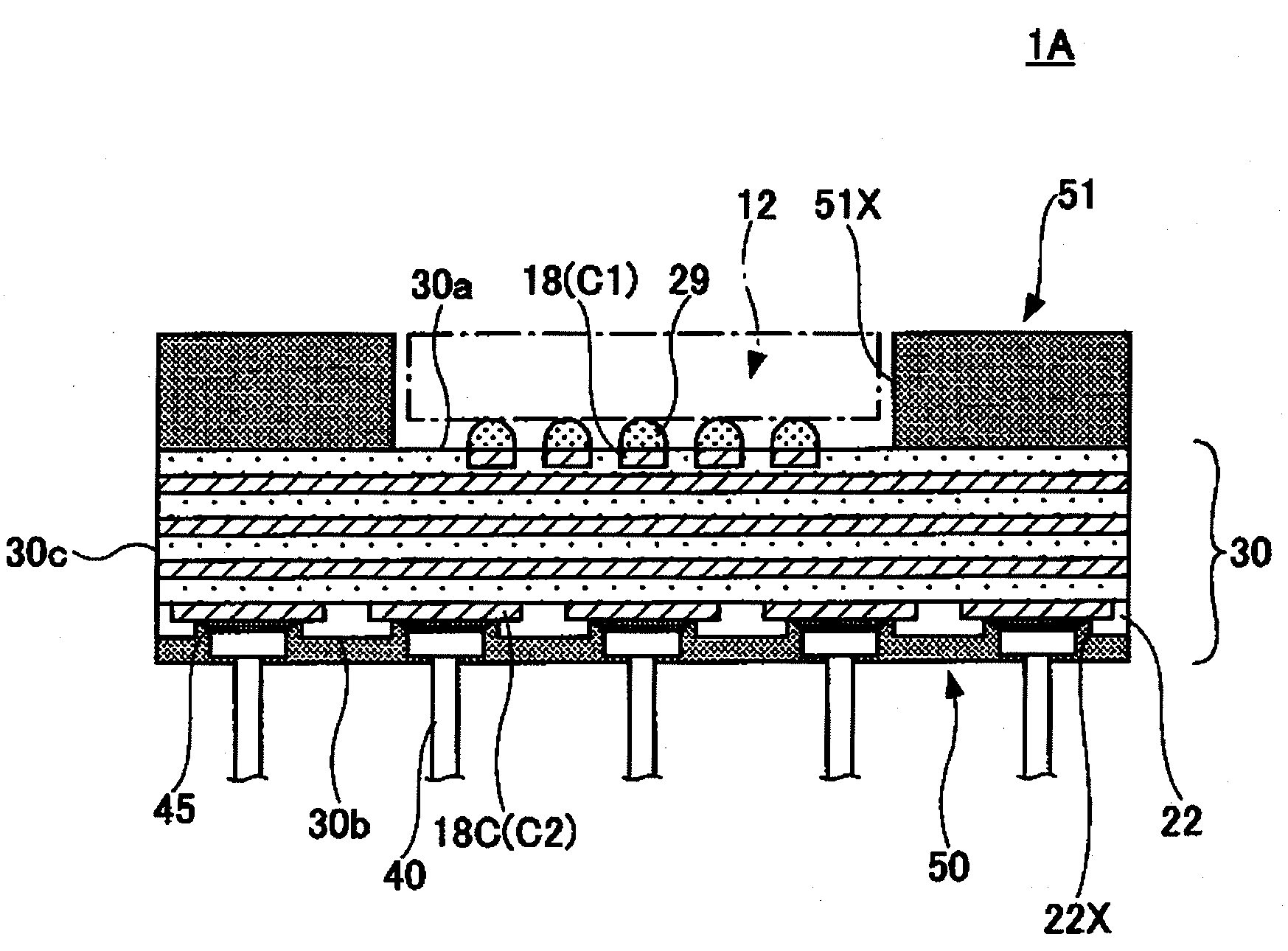
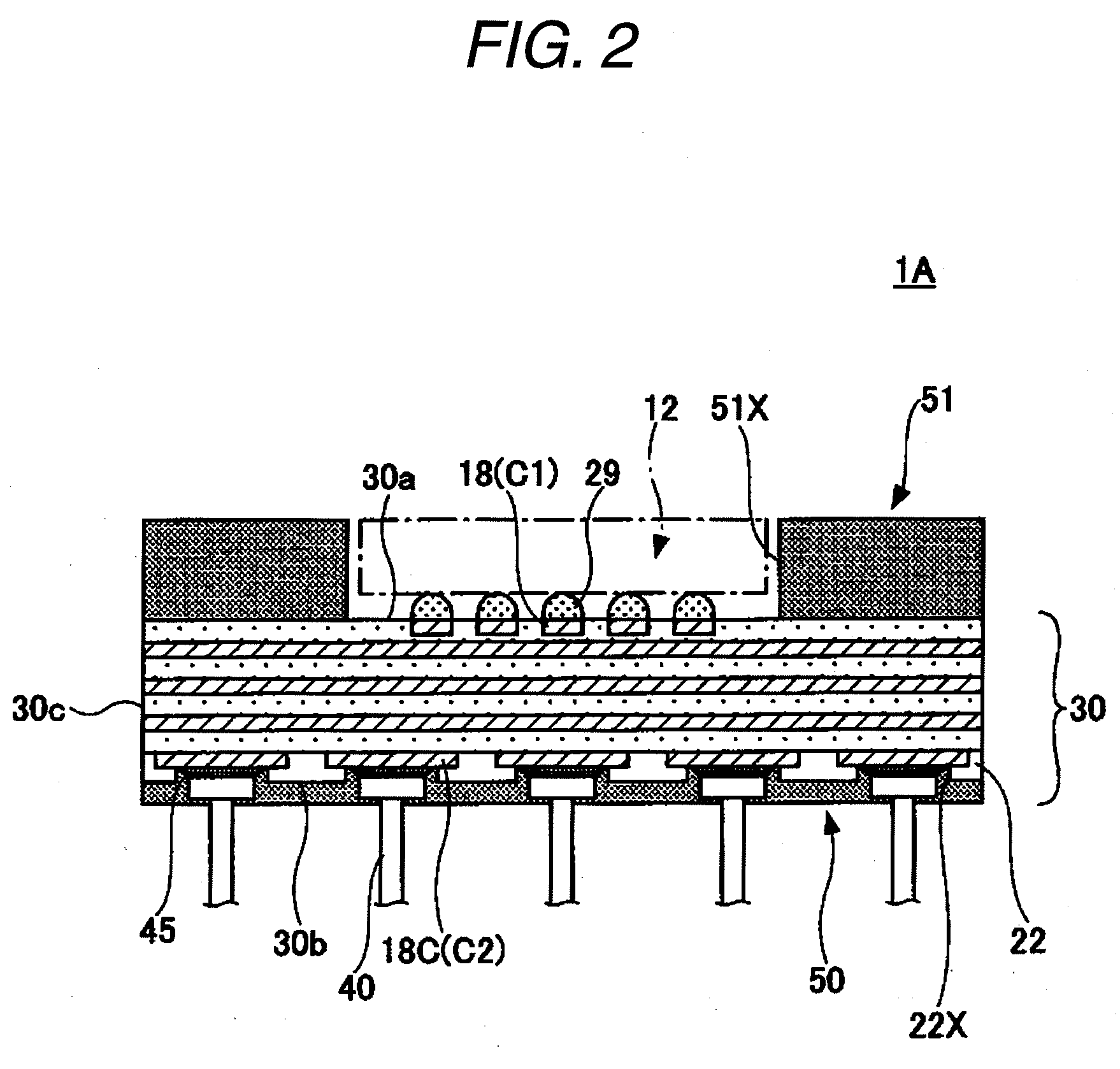
[0066]FIG. 2 is a view typically showing a wiring board 1A according to the invention. The wiring board 1A according to the embodiment is roughly constituted by a wiring member 30, a first reinforcing member 50, and a second reinforcing member 51. The wiring member 30 has a structure in which insulating layers and wiring layers are stacked as will be described below in detail in a process for manufacturing the wiring board 1A (see FIG. 5C).

[0067]A solder bump 29 connected to a first wiring layer 18 to be a first connecting terminal C1 (which will also be referred to as a connecting pad 18 in the description) is disposed on a surface 30a of the wiring member 30. Moreover, a solder resist 22 is formed on a back surface of the wiring member 30, and an opening portion 22X is provided on the solder resist 22. A fourth wiring layer 18c (the second connecting electrode) to be a second connecting terminal C2 is positioned in the opening portion 22X.

[0068]A pin 40 is bonded to the fourth wir...

second embodiment

[0116]In order to manufacture the wiring board 1B having the structure, as shown in FIG. 9A, the chip capacitor 70 is previously provided on the back surface 30b of the wiring board 32 by using the solder 45. The chip capacitor 70 is a small-sized chip-shaped component. Even if the chip capacitor 70 is provided on the back surface 30b of the wiring member 32, therefore, it is not greatly protruded from the back surface 30b.

[0117]FIG. 9B shows a state in which the wiring member 32 having the chip capacitor 70 provided thereon is attached to the metal mold 19A. In this state, the chip capacitor 70 is positioned in a cavity 19h on a lower side and a gap is formed between an internal wall of the cavity 19h and the chip capacitor 70.

[0118]When the wiring member 32 is attached to the metal mold 19A, thus, the same treatment for injecting, into the metal mold 19A, the molding resin 60 as that described with reference to FIGS. 6C and 7 is executed so that the first and second reinforcing ...

seventh embodiment

[0146]In order to manufacture the wiring board 1G having the structure, as shown in FIG. 20, the wiring member 32 having the chip capacitor 70 provided thereon is attached to a metal mold 19A. In this state, the chip capacitor 70 is positioned in a cavity 19h on a lower side and a gap is formed between an internal wall of the cavity 19h and the capacitor 70. Furthermore, a projecting portion 19f formed on a lower mold 19b is set into an abutting state on the fourth wiring layer 18c of the wiring member 30.

[0147]When the wiring member 32 is attached to the metal mold 19A, thus, processings in FIGS. 17C, 18A and 18B are executed so that the wiring board 1G shown in FIG. 19 is manufactured. Even if the chip capacitor 70 is provided on the wiring member 32, thus, the wiring board 1G can be manufactured by the same molding method as that in the fifth and sixth embodiments.

[0148]Next, description will be given to a wiring board and a method of manufacturing the wiring board according to ...


PUM

PropertyMeasurementUnit
heightaaaaaaaaaa
heightaaaaaaaaaa
heightaaaaaaaaaa

Abstract

A wiring board has a wiring member, a first reinforcing member and a second reinforcing member. The wiring member has wiring layers and insulating layers which are stacked, and the wiring layers include a first connecting electrode formed on a surface of the wiring member and a second connecting electrode formed on a back surface of the wiring member. A pin is formed on the second connecting electrode. The second reinforcing member is formed by a resin and serves to reinforce the wiring member. The first reinforcing member is formed on the whole back surface of the wiring member except for the pin provided on the second connecting electrode.

Description

TECHNICAL FIELD[0001]The present disclosure relates to a wiring board and a method of manufacturing the wiring board. More specifically, the present disclosure relates to a wiring board in which a reinforcing member is provided on a wiring member formed by stacking a wiring layer and an insulating layer on a support and then removing the support, and a method of manufacturing the wiring board.RELATED ART[0002]In a wiring board to be used in a semiconductor package, there has been used a build-up wiring board having a wiring board and an insulating layer, which are stacked on both upper and lower surfaces of a core board in order to increase a density of a wiring pattern.[0003]However, an increase in a density of a semiconductor chip to be provided has progressed. For a build-up wiring board, there has been given a request for a further increase in a density of a wiring pattern and a further reduction in a thickness of a wiring board. In order to meet the request, there has been deve...

Claims


Application Information

Patent Timeline
Patent Type & Authority Applications(United States)
IPC IPC(8): H05K1/11H05K3/00
CPCH01L21/481Y10T29/49124H01L23/49811H01L23/49822H01L23/49861H01L24/16H01L2221/68345H01L2224/16H01L2924/01046H01L2924/01078H01L2924/01079H01L2924/15153H01L2924/1517H01L2924/15174H01L2924/15312H01L2924/1815H01L2924/19041H01L2924/19042H01L2924/19043H01L2924/19106H01L2924/3511H05K3/284H05K2201/09136H05K2201/10318H05K2201/10977H05K2203/1316H01L21/6835H05K1/02
Inventor MATSUSHITA, YOSHITAKAOSHIMA, KAZUHIROHORIUCHI, AKIO
Owner SHINKO ELECTRIC IND CO LTD
Why Eureka
Try Eureka