Method to form CMOS circuits with sub 50nm sti structures using selective epitaxial silicon post sti etch

Inactive Publication Date: 2009-04-16
TEXAS INSTR INC
View PDF7 Cites 34 Cited by
  • Summary
  • Abstract
  • Description
  • Claims
  • Application Information

AI Technical Summary

Benefits of technology

[0005]The instant invention provides an improved shallow trench isolation (STI) element of field oxide in an integrated circuit (IC) which includes a layer of epitaxial semiconductor on sidewalls of the STI trench which increase the width of the active area in the IC adjacent to the STI trench and decreases a width of dielectric material in the STI trench. A pre-epitaxial growth cleanup process removes STI etch residue from the STI trench surface. The epitaxial semiconductor composition is matched to the composit

Problems solved by technology

STI processes include etches and oxidation operations which typically consume 10 nanometers or more of silicon on each side of an element of field oxide, undesirably reducing the silicon to field oxide ratio belo

Method used


Image

  • Method to form CMOS circuits with sub 50nm sti structures using selective epitaxial silicon post sti etch
  • Method to form CMOS circuits with sub 50nm sti structures using selective epitaxial silicon post sti etch
  • Method to form CMOS circuits with sub 50nm sti structures using selective epitaxial silicon post sti etch

Examples


Embodiment Construction

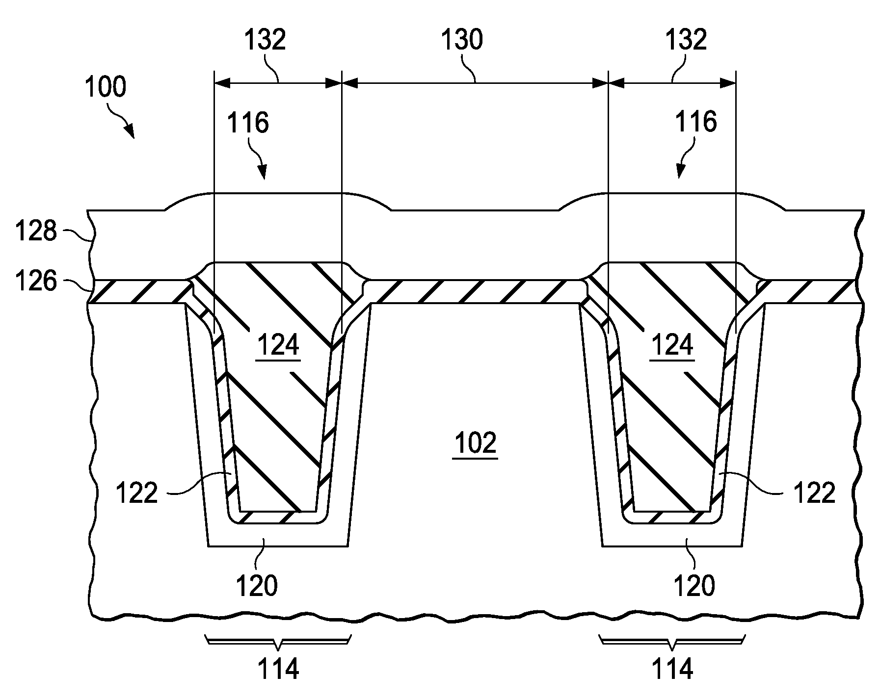
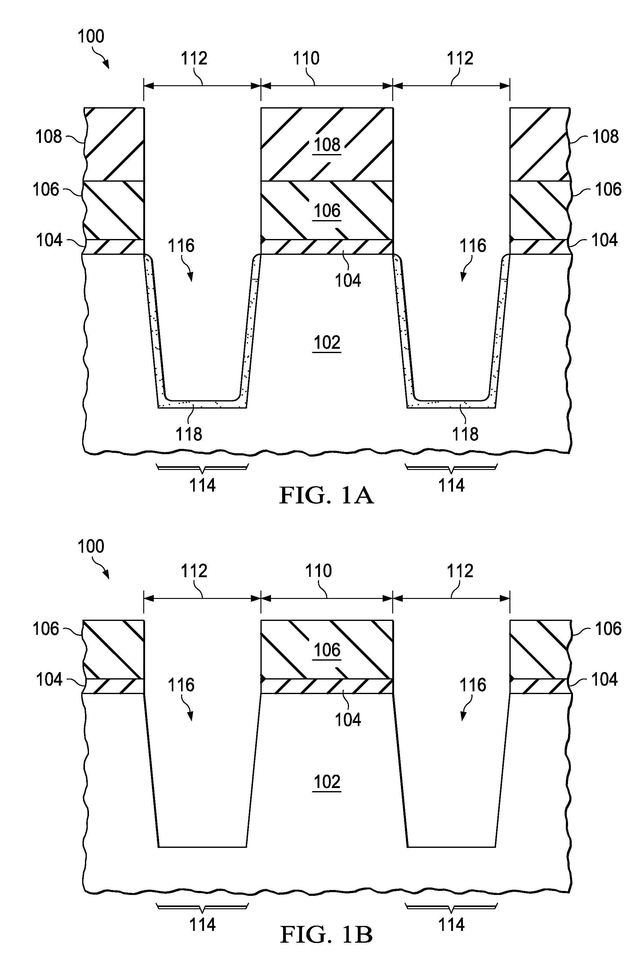
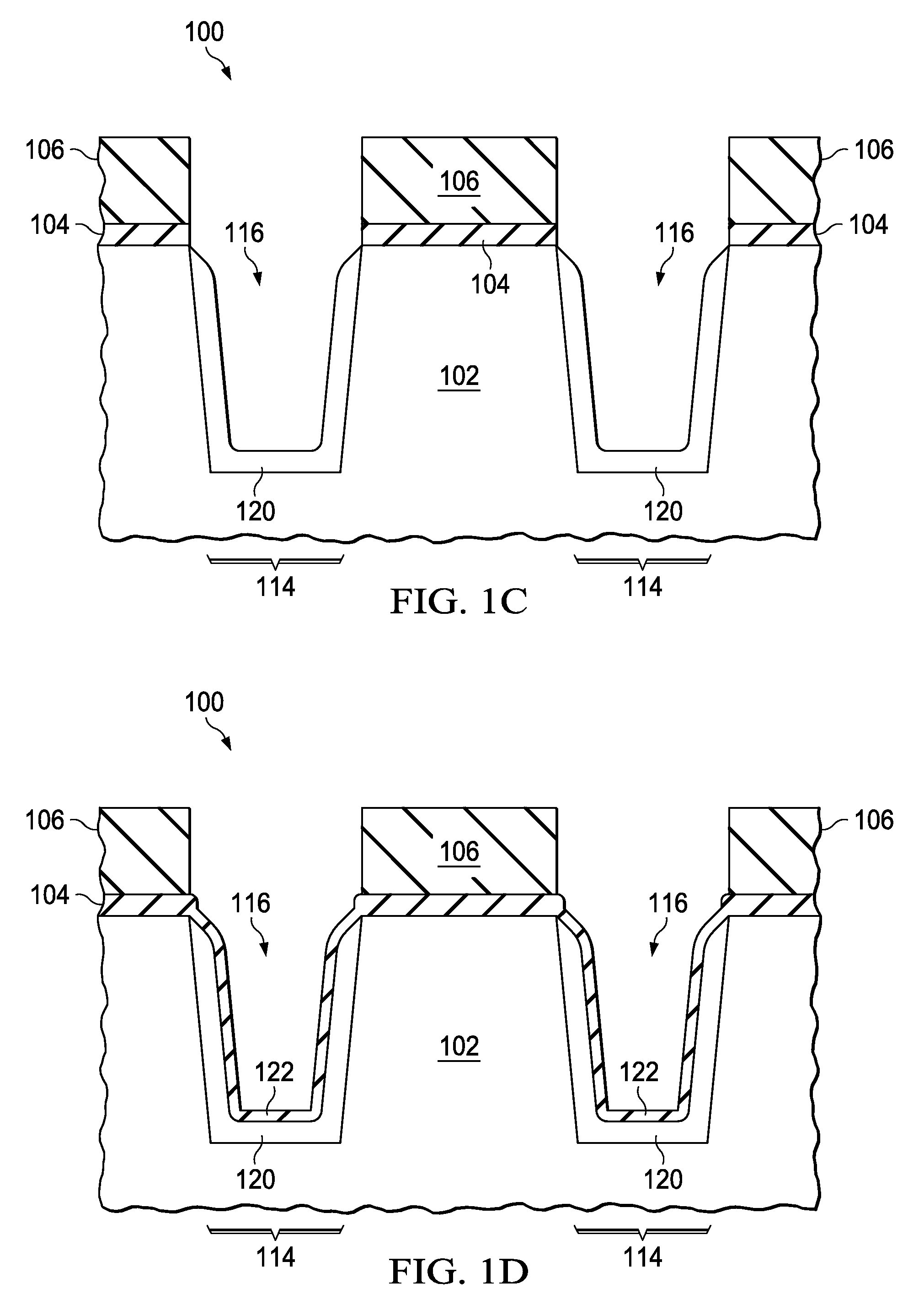
[0008]The present invention is described with reference to the attached figures, wherein like reference numerals are used throughout the figures to designate similar or equivalent elements. The figures are not drawn to scale and they are provided merely to illustrate the invention. Several aspects of the invention are described below with reference to example applications for illustration. It should be understood that numerous specific details, relationships, and methods are set forth to provide a full understanding of the invention. One skilled in the relevant art, however, will readily recognize that the invention can be practiced without one or more of the specific details or with other methods. In other instances, well-known structures or operations are not shown in detail to avoid obscuring the invention. The present invention is not limited by the illustrated ordering of acts or events, as some acts may occur in different orders and / or concurrently with other acts or events. F...


PUM


Abstract

An STI field oxide element in an IC which includes a layer of epitaxial semiconductor on sidewalls of the STI trench to increase the width of the active area adjacent to the STI trench and decrease a width of dielectric material in the STI trench is disclosed. STI etch residue is removed from the STI trench surface prior to growth of the epitaxial layer. The epitaxial semiconductor composition is matched to the composition of the adjacent active area. The epitaxial semiconductor may be undoped or doped to match the active area. The STI trench with the epitaxial layer is compatible with common STI passivation and fill processes. The thickness of the as-grown epitaxial semiconductor layer is selected to provide a desired active area width or a desired STI dielectric width.

Description

FIELD OF THE INVENTION[0001]This invention relates to the field of integrated circuits. More particularly, this invention relates to methods to improve shallow trench isolation.BACKGROUND OF THE INVENTION[0002]It is well known that lateral dimensions of components in advanced complementary metal oxide semiconductor (CMOS) integrated circuits (ICs) are shrinking with each new fabrication technology node, as articulated by Moore's Law. Transistors in CMOS ICs are electrically isolated from each other by elements of field oxide formed by shallow trench isolation (STI) processes. In dense circuits of conventional planar metal oxide semiconductor (MOS) transistors, it is desirable to have a width ratio of silicon to field oxide above 0.85:1 with field oxide between 250 to 350 nanometers thick. In dense circuits of three dimensional transistors, commonly known as finFETs, it is desirable to have a width ratio of silicon to field oxide above 1.5:1 with isolation trenches between 100 and 15...

Claims


Application Information

Patent Timeline
IPC IPC(8): H01L21/762H01L23/00
CPCH01L21/76232
Inventor MONTGOMERY, CLINT L.KIRKPATRICK, BRIAN K.XIONG, WEIZEPRINS, STEVEN L.
Owner TEXAS INSTR INC
Why Eureka
Try Eureka