Tenon-and-mortise packaging structure

Active Publication Date: 2009-04-16
ADVANCED SEMICON ENG INC
View PDF1 Cites 5 Cited by
  • Summary
  • Abstract
  • Description
  • Claims
  • Application Information

AI Technical Summary

Benefits of technology

[0008]According to a first aspect of the present invention, a tenon-and-mortise packaging structure is provided. A tenon projection and a corresponding mortise slot are formed on two opposite surfaces of a substrate for coupling two or more substrates to form a stacked package structure. Also, a plurality of conduction portions are electroplated on the surface of the tenon projection and the inner side of the mortise slot for electrically connecting between the substrates of a stacked package structure when the substrates are jointed to each other by coupling the tenon projections to a corresponding mortise slots, without additional device for electrical connection, hence largely reducing the circuit required space.
[0009]According to a second aspect of the present invention, a tenon-and-mortise packaging structure including a substrate is provided. The substrate has a top surface and a corresponding lower surface. The top surface forms at least one tenon projection, and the lower surface forms at least one mortise slot corresponding to the tenon projection in shape and position. When the two substrates are stacked on each other, the tenon projection can be inserted into the mortise slot and engaged with the mortise slot through the interference for coupling the two substrates together to form a stacked structure. In other words, according to the invention, two substrates are precisely positioned by the engaging mechanism between the mortise slot and the tenon projection which are disposed on the top and the lower surfaces of the substrate, hence avoiding the defects in positioning which may occur when the substrates are stacked on one another by an adhesive according to generally known techniques.
[0010]According to a third aspect of the present invention, a tenon-and-mortise packaging structure including a plurality of substrates is provided. Each substrate has a top surface and a lower surface opposite to the top surface. The top and the lower surfaces of the substrate respectively form a mortise slot and a tenon projection. A plurality of substrates can be stacked on one another and jointed to each other to form a stacked package by coupling the mortise slot to a tenon projection. The inner and outer surfaces of the mortise slot and the tenon projection are respectively electroplated with a conduction portion for electrically connecting two neighboring substrates when the substrates are vertically stacked on one another to form a stacked package by coupling the mortise slot to the tenon projection, largely reducing the required circuit space for the stacked package and enhancing the electrical properties.
[0011]According to a fourth aspect of the present invention, a tenon-and-mortise packaging structure including a carrier is provided. The carrier has a top surface and a lower surface opposite to top surface. The top and the lower surfaces of the carrier respectively form a mortise slot and a tenon projection corresponding to the mortise slot in shape and position. A chip, embedded in the carrier by the way of vacuum, has an active surface and a back side opposite to the active surface. The active surface of the chip is eclectically connected with the tenon projection disposed on the top surface of the carrier via a plurality of wires embedded in the carrier. The back side of the chip is also electrically connected with the mortise slot disposed on the lower surface of the carrier via the wires embedded in the carrier. As the chip is embedded in the carrier by the way of vacuum and is electrically connected with the top and the lower surfaces of the carrier via the wires embedded in the carrier, there is no need to provide a dielectric layer disposed between the chip and the carrier, hence avoiding the non-uniformity problem of spin-coating the dielectric layer which occurs when conventional techniques are employed thus increasing the yield rate of CIP package.
[0012]A stacked package with precise positioning is formed via coupling a mortise slot and a corresponding tenon projection which are disposed on two opposite surfaces of a substrate (carrier) so that defects in positioning are avoided, the space required for forming electrical connection in the stacked package is reduced, the electrical properties are enhanced, and the volume of the package structure is reduced. As the dielectric layer is dispensed, the stacked package formed by the tenon-and-mortise packaging structure of the invention is free of the non-uniformity problem which occurs when the dielectric layer is spin-coated.

Problems solved by technology

However, the problem in the manufacturing process of CIP package is the yield rate to be desided by uniformity of the dielectric layer.
As the dielectric layer is formed via spin-coating and then bring about a micro-porous structure after exposure and developing process, the uniformity of the dielectric layer becomes very hard to control during the manufacturing process, hence affecting the yield rate of CIP package.
However, after repeated heating cycling in the manufacturing process, the adhesive may be detached and come off.
Besides, during the stacking process, the yield rate of the package will be affected if the substrates are not positioned precisely.

Method used


Image

  • Tenon-and-mortise packaging structure
  • Tenon-and-mortise packaging structure
  • Tenon-and-mortise packaging structure

Examples


Embodiment Construction

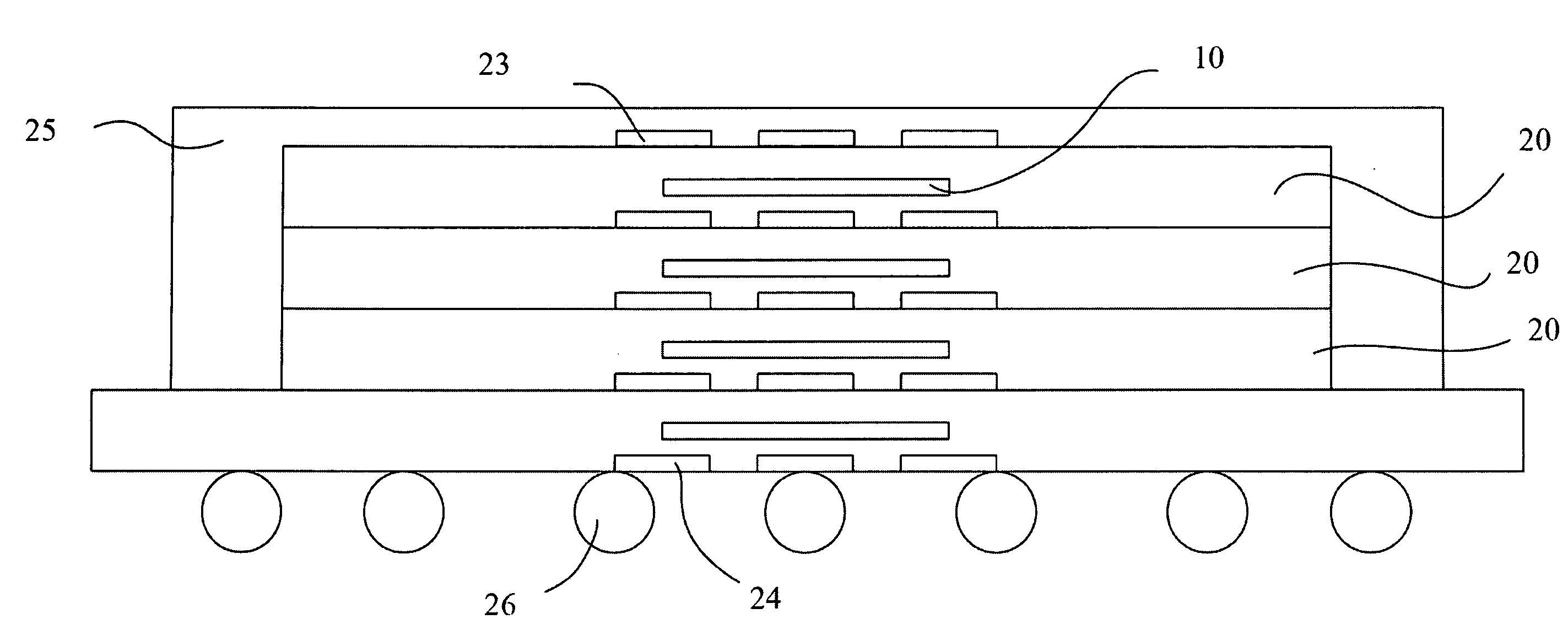
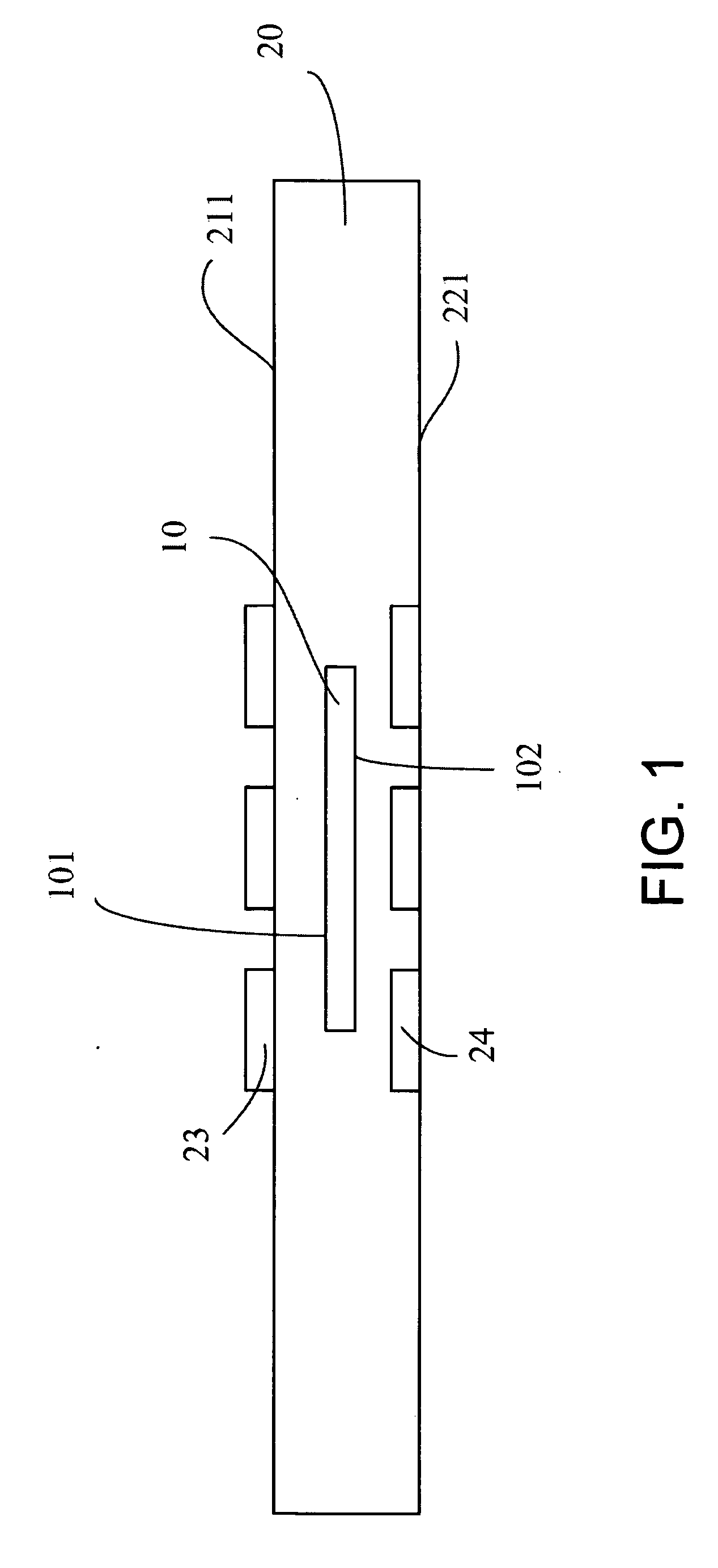
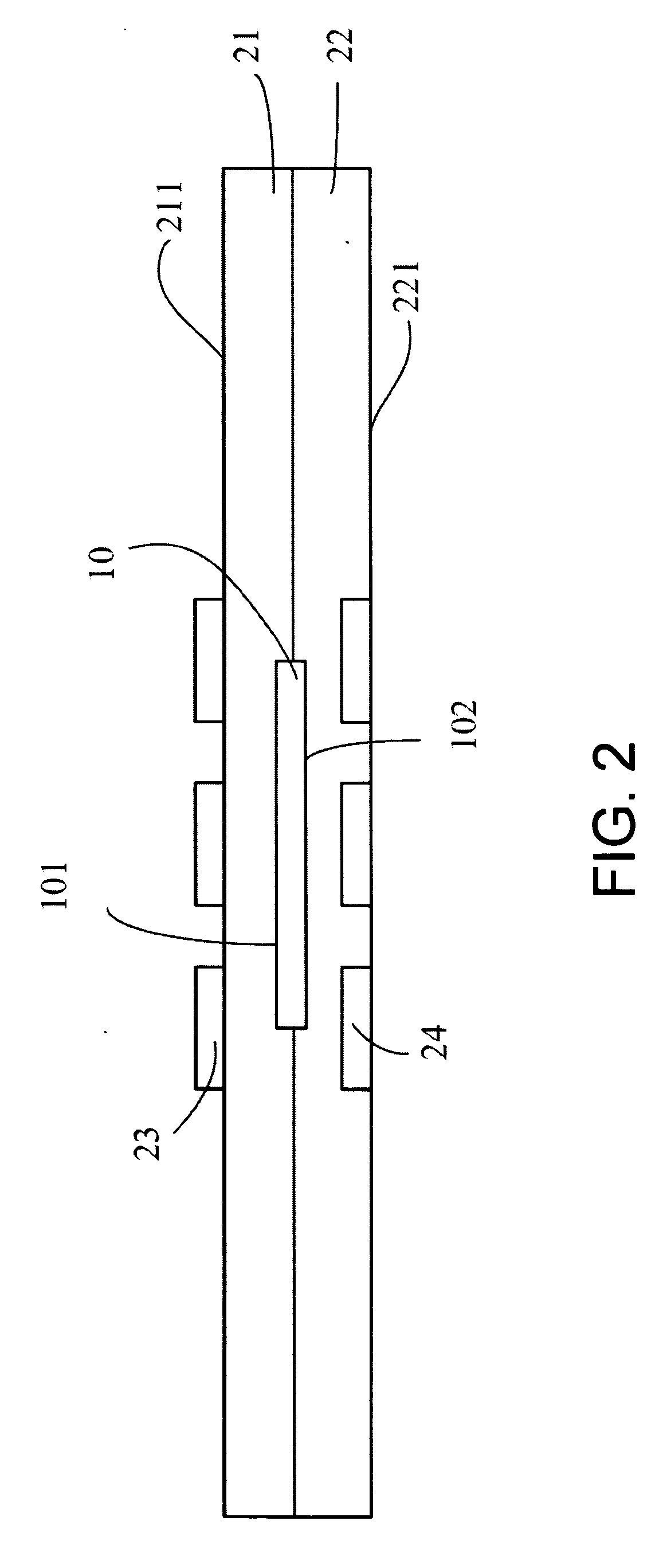
[0018]The tenon-and-mortise packaging structure of the invention is disclosed below with accompanying drawings. FIG. 1 shows a perspective of a tenon-and-mortise packaging structure according to a preferred embodiment of the invention. As indicated in FIG. 1, the tenon-and-mortise packaging structure includes a carrier 20 exemplified as a substrate in the present embodiment of the invention. However, the carrier 20 is not limited to a substrate and can be implemented by any suitable structures or components.

[0019]The carrier 20 has a top surface (or top surface 211) and a bottom surface (or lower surface 221) opposite to the top surface. The defining words “top” and “lower” refer to the relative position in the related drawings and are irrelevant to actual position of the carrier 20 or the tenon-and-mortise packaging structure of the invention. In the present embodiment of the invention, the top surface 211 opposite to the lower surface 221, and it is only one of the implementations...


PUM


Abstract

A tenon-and-mortise packaging structure including a carrier and a chip is provided. The carrier has a top surface and a lower surface opposite to the top surface. The top surface forms at least one tenon projection, and the lower surface forms a mortise slot corresponding to the tenon projection in shape, size, and position, so that two carriers can be stacked on and jointed to each other by coupling the tenon projection to the corresponding mortise slot. The tenon projection and the mortise slot have conduction portions, respectively. When the tenon projection and the mortise slot are engaged with each other, the conduction portions are electrically connected with each other. At least one chip is embedded in the carrier. The chip has an active surface and a back side respectively and electrically connected with the top and the lower surfaces of the carrier.

Description

[0001]This application claims the benefit of Taiwan application Serial No. 96138714, filed Oct. 16, 2007, the subject matter of which is incorporated herein by reference.BACKGROUND OF THE INVENTION[0002]1. Field of the Invention[0003]The invention relates in general to a tenon-and-mortise packaging structure and a manufacturing method thereof, and more particularly to a packaging structure which achieves precise positioning of stacked package by a CIP package.[0004]2. Description of the Related Art[0005]With the rapid progress in electronic products, the integrated circuit (IC) has become an indispensible product in information age and has been widely used in electronic devices such as notebook computer, mobile phone, personal digital assistant (PDA) and digital camera. In terms of the chip package structure of an electronic product, the electronic product must not only have as many active elements as possible to meet the requirements of multi-function and high-speed and high-freque...

Claims


Application Information

Patent Timeline
IPC IPC(8): H01L21/00H01L23/02
CPCH01L23/3107H01L25/03H01L2225/0652H01L2225/06555H01L2225/06586H01L2924/0002H01L2924/15311H01L25/16H01L2924/00
Inventor LAI, YI-SHAOTSAI, TSUNG-YUEHCHANG, HSIAO-CHUANCHEN, TSAN-HSIEN
Owner ADVANCED SEMICON ENG INC
Why Eureka
Try Eureka