Supercharge Your Innovation With Domain-Expert AI Agents!

Optical interconnect system providing communication between computer system components

a computer system and interconnection technology, applied in the field of optical interconnection, can solve the problems of limiting the maximum number of dimms per channel, unable to meet the demands of current and future multi-core microprocessors, and unable to scale with the demands of multi-core microprocessors

Active Publication Date: 2009-04-16
HEWLETT-PACKARD ENTERPRISE DEV LP
View PDF12 Cites 29 Cited by
  • Summary
  • Abstract
  • Description
  • Claims
  • Application Information

AI Technical Summary

Benefits of technology

[0007]The present invention provides one or more embodiments of an optical interconnect system for communication between computer system components. In one embodiment, the optical interconnect system comprises an optical data communication path and a plurality of optical taps, each optical tap optically coupling a respective computer system component to the optical data communication path. Each optical tap splits power of a signal received from either the optical data communication path or its respective computer component into an optical signal having a first power and an optical signal having a second power in accordance with a respective power ratio relationship between reflectivity and transmissivity. The ratio relationships of the optical taps together provide a predetermined communication reliability as determined by a metric for signals traversing the optical interconnect system between computer system components.

Problems solved by technology

Electrical communication architectures struggle to balance the dichotomy for increased performance required of electronic systems while addressing lower power consumption, smaller form factor, and lower electromagnetic emissions.
This parallel bus architecture has reached a point where it can no longer scale with the demands of current and future multi-core microprocessors.
In a typical example of bulk memory using Dual In-line Memory Module (DIMM) technology with a series of Dynamic Random Access Memory (DRAM) integrated circuits in each DIMM mounted on a printed circuit board (PCB), the electrical problem of scaling the high-speed parallel bus to wider widths and speeds limit the maximum number of DIMMs per channel.
However, the daisy chaining or point-to-point configuration is problematic as the hops introduce latency.
The need to replicate and forward both northbound and southbound signals adds latency, eventually leading to bottlenecks.
The AMBs also consume a large amount of power due to the need to send the high speed electrical signals between AMBs and the serialization and deserialization of data from the DIMMs.
These examples illustrate that, as the speed of communication in electrical systems has increased, signal integrity issues have limited electrical communication memory interconnects to point-to-point interconnects.

Method used


Image

  • Optical interconnect system providing communication between computer system components
  • Optical interconnect system providing communication between computer system components
  • Optical interconnect system providing communication between computer system components

Examples


Embodiment Construction

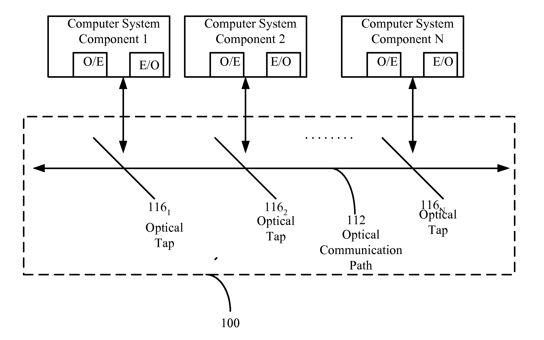
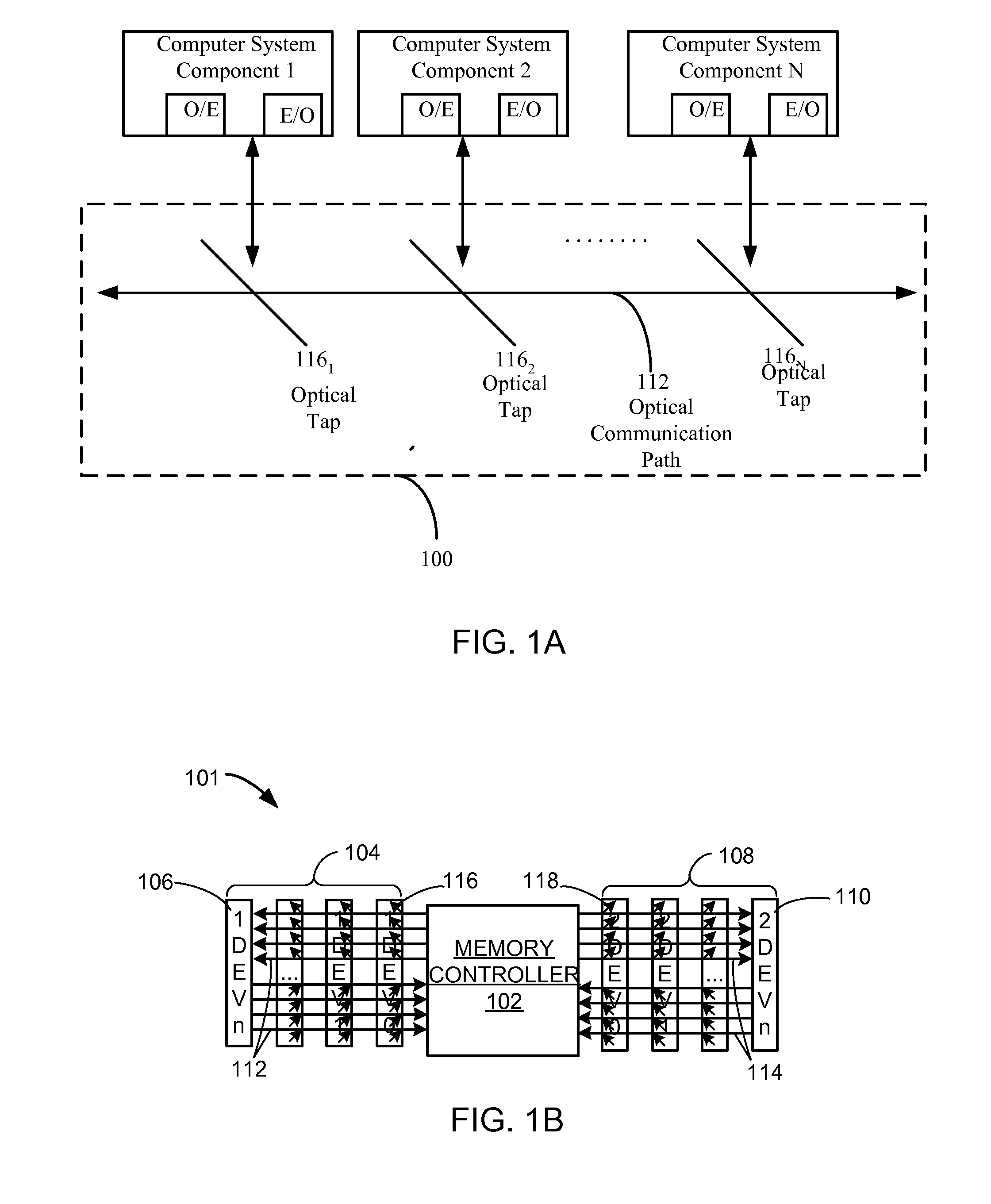
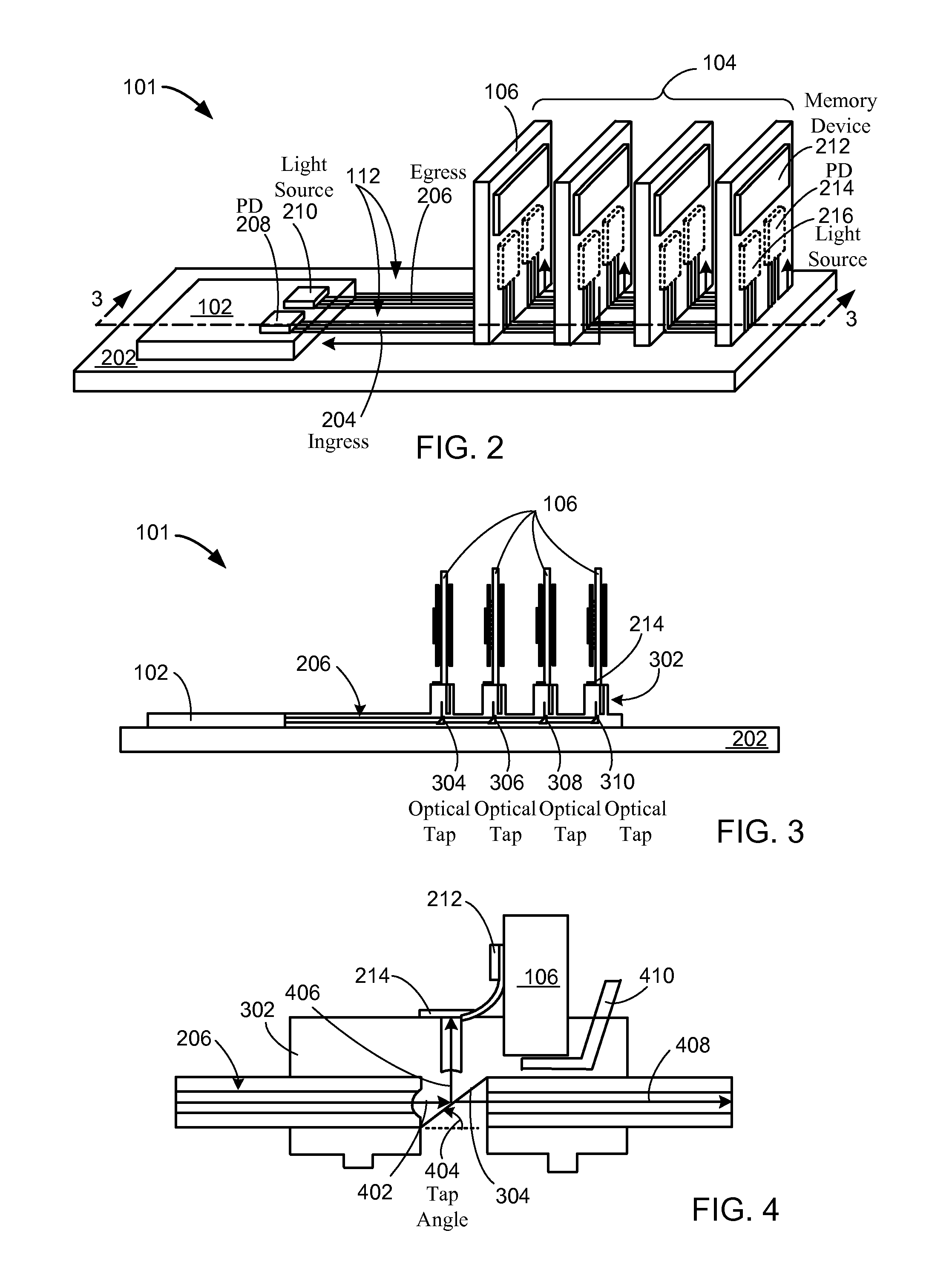
[0019]The following embodiments are described in sufficient detail to enable those skilled in the art to make and use the invention. It is to be understood that other embodiments would be evident based on the present disclosure, and that system, process, or mechanical changes may be made without departing from the scope of the present invention.

[0020]In the following description, numerous specific details are given to provide a thorough understanding of the invention. However, it will be apparent that the invention may be practiced without these specific details. The drawings showing embodiments of the system are semi-diagrammatic and not to scale and, particularly, some of the dimensions are for the clarity of presentation and are shown greatly exaggerated in the drawing FIGS.

[0021]In addition, where multiple embodiments are disclosed and described having some features in common, for clarity and ease of illustration, description, and comprehension thereof, similar and like features...


PUM


Abstract

An optical interconnect system for communication between computer system components is described. The system includes an optical data communication path and a plurality of optical taps, each optical tap optically coupling a respective computer system component to the optical data communication path. Each optical tap splits power from an optical signal received from the data communication path or from a light source generating a data signal from its associated computer component resulting in another optical signal. Each optical tap splits light in accordance with a respective power ratio relationship between reflectivity and transmissivity. The ratio relationships of the optical taps together provide a predetermined communication reliability metric for signals traversing the optical interconnect system between computer system components.

Description

TECHNICAL FIELD[0001]The present invention relates generally to an optical interconnect which provides communication between computer system components. For example, the optical interconnect provides optical communication between a memory controller and memory devices.BACKGROUND ART[0002]Electrical communication architectures struggle to balance the dichotomy for increased performance required of electronic systems while addressing lower power consumption, smaller form factor, and lower electromagnetic emissions. Better solutions dealing which address scalability while reducing power consumption in computer systems is desirable. A memory system is an example of a typical computer system in which such better solutions are desirable.[0003]Some current computer memory systems use a wide parallel bus to communicate with bulk memory. With increasing memory densities and memory bus speeds, the bus widths and speeds must also be increased. This parallel bus architecture has reached a point...

Claims


Application Information

Patent Timeline
IPC IPC(8): H04J14/02H04B10/2581
CPCH04J14/02H04B10/803
Inventor TAN, MICHAEL RENNEMORRIS, TERRELJOUPPI, NORMAN PAULWANG, SHIH-YUAN
Owner HEWLETT-PACKARD ENTERPRISE DEV LP
Features
  • R&D
  • Intellectual Property
  • Life Sciences
  • Materials
  • Tech Scout
  • Unparalleled Data Quality
  • Higher Quality Content
  • 60% Fewer Hallucinations
Learn More