Image detector

Active Publication Date: 2009-04-23
FUJIFILM CORP
View PDF3 Cites 0 Cited by
  • Summary
  • Abstract
  • Description
  • Claims
  • Application Information

AI Technical Summary

Benefits of technology

[0020]According to the image detector of the present invention, the insulating bonding member is bonded to the active matrix substrate through the inorganic insulating film disposed in an area around the periphery of the semiconductor layer, so that the adhesiveness between the insulating bonding member and active matrix substrate may be improved. Therefore, detachment of the insulating bonding member due to linear expansion when a temperature change occurs may be prevented, whereby line breakages arising from creeping discharges and the like may be prevented properly. Further, the improvement of the adhesiveness between the insulating bonding member and active matrix substrate allows the protection substrate, which is bonded to the active matrix substrate through the insulating bonding member, to be adequately bonded to the active matrix substrate.
[0021]In the image detector of the present invention, the protection substrate and active matrix substrate are temporarily bonded by an adhesive, and where the protection substrate is bonded to the active matrix substrate through an organic insulating film

Problems solved by technology

Where the bonding strength between the resin material 119 and TFT array substrate 100 in the image detector of Japanese Patent No. 3737343 is insufficient, however, a detachment problem arises at the interface between the resin material and TFT array substrate 100 by linear expansion due to temperature change, which will lead to creeping discharges or wire breakages.
It has been found that, where the up

Method used


Image

  • Image detector
  • Image detector
  • Image detector

Examples


first embodiment

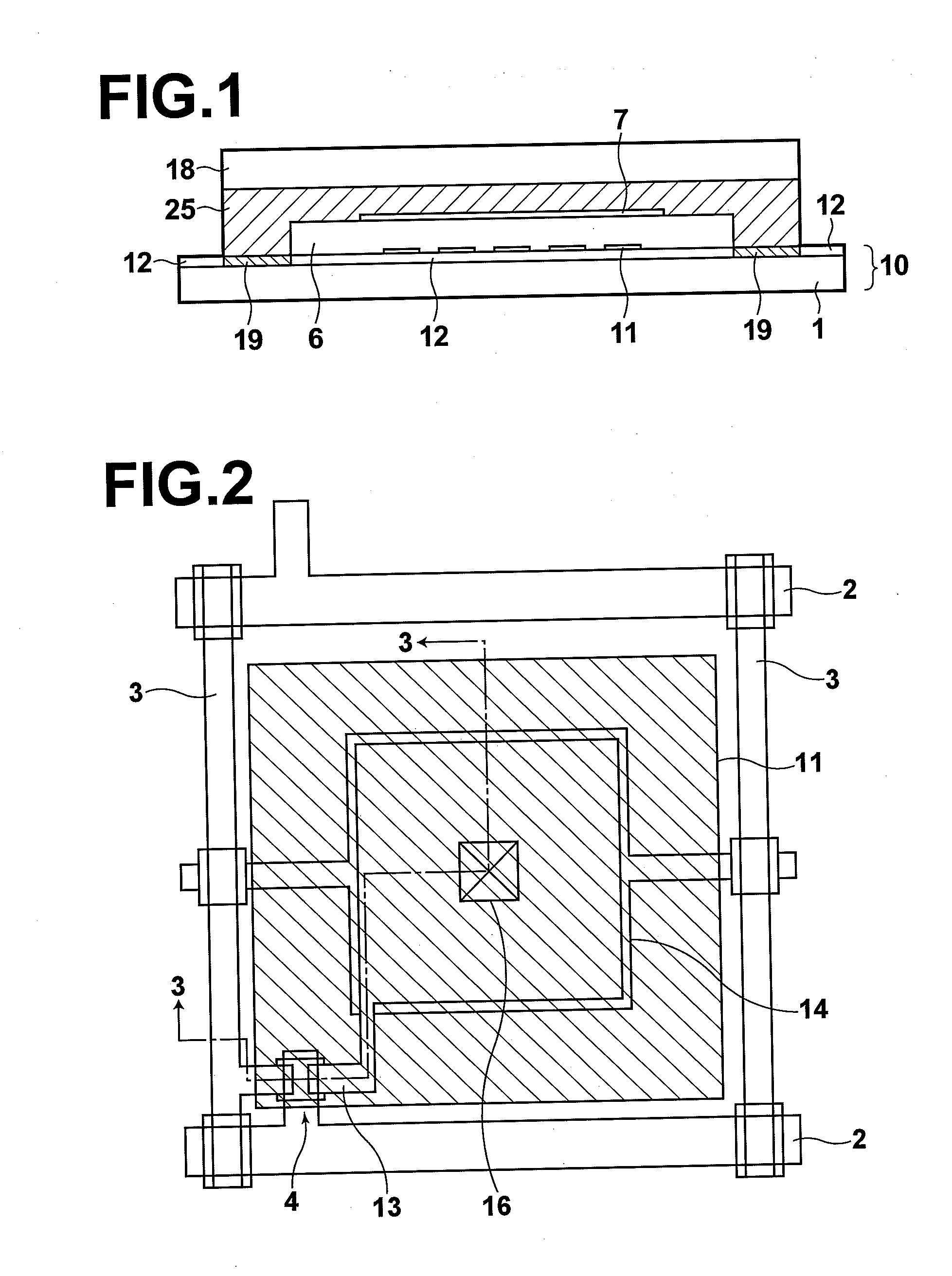
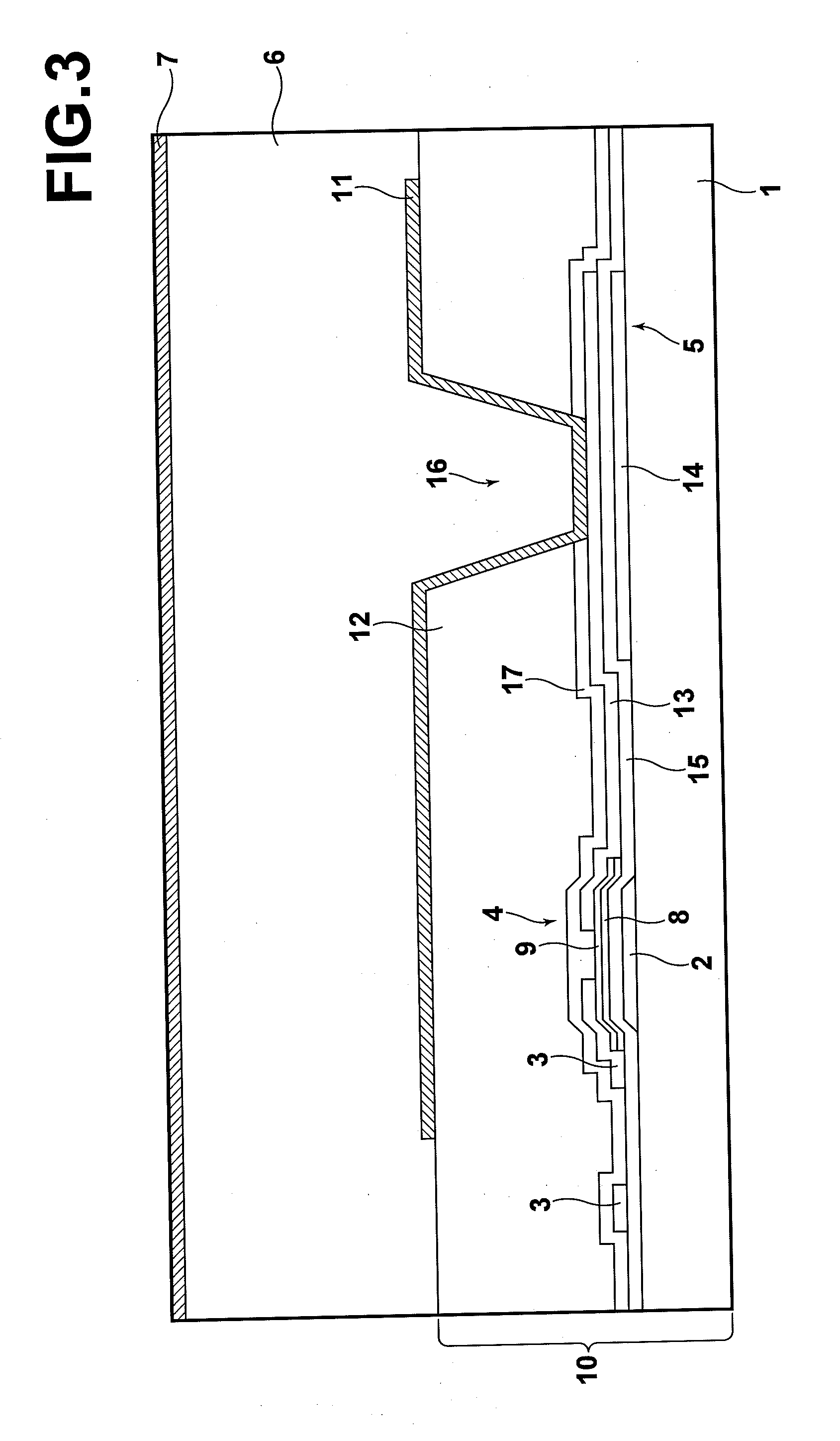
[0041]Hereinafter, a radiation image detector to which is applied the image detector of the present invention will be described with reference to the accompanying drawings. FIG. 1 illustrates a schematic structure of the radiation image detector.

[0042]As illustrated in FIG. 1, the radiation image detector includes a TFT array substrate 10 having a substrate on which multitudes of TFT switches are disposed, a semiconductor layer 6 which generates charges according to an electromagnetic wave representing a radiation image irradiated thereon and is stacked on the TFT array substrate 10 such that the charges are read out by the TFT array substrate 10, an upper electrode 7 stacked on the semiconductor layer 6, an insulating bonding member 25 provided so as to cover a peripheral portion of the semiconductor layer 6 and an upper portion of the upper electrode 7 and to bond a protection substrate 18, to be described later, with the TFT array substrate 10, and the protection substrate 18 sta...

second embodiment

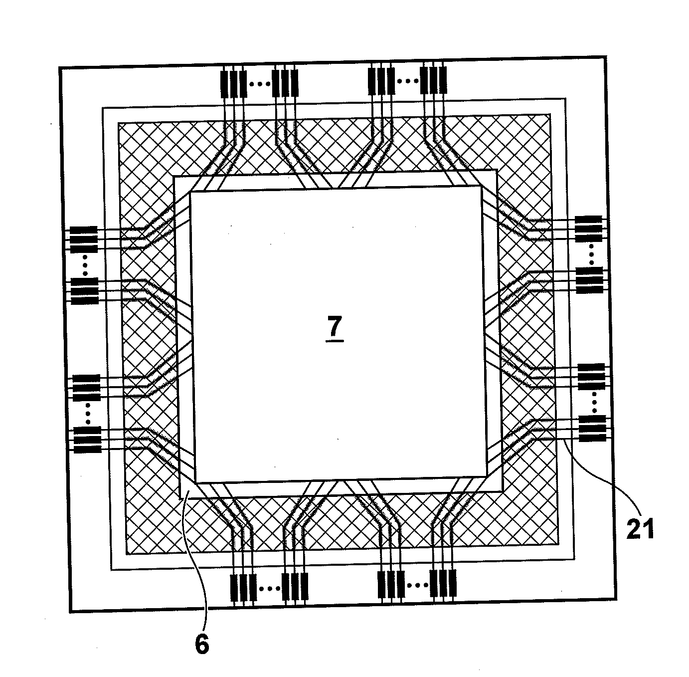
[0066]Also in the radiation image detector of the second embodiment, an inorganic insulating film 19 is provided at the entire bonding area of the insulating bonding member 25 to the TFT array substrate 10 in order to improve the adhesiveness between the insulating bonding member 25 and TFT array substrate 10. The inorganic insulating film 19 is provided so as to enclose the semiconductor layer 6. FIG. 6 is a top view illustrating the area where the inorganic insulating film 19 is provided.

[0067]The other structure of the radiation image detector of the second embodiment is identical to that of the radiation image detector of the first embodiment.

[0068]Next, a method of manufacturing the radiation image detector of the second embodiment will be described with reference to FIGS. 7A to 7F.

[0069]First, as illustrated in FIG. 7A, a TFT array substrate 10 is formed. Here, an interlayer insulating film 12 is formed through patterning by photolithography so as not to be formed in an area s...

third embodiment

[0084]Thus, in the radiation image detector of the third embodiment, the inorganic insulating film 19 is formed on the entire surface of the TFT array substrate 10, and the underlayer 20 is bonded to the TFT array substrate 10 through the inorganic insulating film 19, as illustrated in FIG. 8. By disposing the inorganic insulating film 19 in the manner as described above, the adhesiveness between the underlayer 20 and TFT array substrate 10 may be improved.

[0085]Also in the radiation image detector of the third embodiment, the inorganic insulating film 19 is provided at the entire bonding area of the insulating bonding member 25 to the TFT array substrate 10 in a manner to enclose the semiconductor layer 6 in order to improve the adhesiveness between the insulating bonding member 25 and TFT array substrate 10, as in the second embodiment. FIG. 9 is a top view illustrating the contact area of the inorganic insulating film 19 with the insulating bonding member 25.

[0086]As described ab...


PUM


Abstract

An image detector which includes an active matrix substrate and a protection substrate bonded to the active matrix substrate by an insulating bonding member, in which the insulating bonding member is bonded to the active matrix substrate through an inorganic insulating film disposed in an area around the periphery of the semiconductor layer.

Description

BACKGROUND OF THE INVENTION[0001]1. Field of the Invention[0002]The present invention relates to an image detector having an active matrix substrate with multitudes of switching elements disposed thereon.[0003]2. Description of the Related Art[0004]Recently, a flat panel detector (FPD) has been put into practical use. The FPD includes an active matrix substrate with multitudes of switching elements disposed thereon and an X-ray sensitive layer stacked thereon, and is capable of directly converting X-ray information to digital data. The FPD is advantageous over a conventional imaging plate in that it allows for confirmation of a motion picture, as well as instantaneous confirmation of images.[0005]As one of such FPDs, for example, Japanese Patent No. 3737343 proposes an image detector like that shown in FIG. 17.[0006]The image detector proposed in Japanese Patent No. 3737343 includes a TFT array substrate 100 with multitudes of TFT switches disposed two-dimensionally, a semiconductor...

Claims


Application Information

Patent Timeline
IPC IPC(8): H01L27/088
CPCG01T1/2928H01L27/14676H01L27/14618H01L2924/0002H01L2924/00
Inventor OKADA, YOSHIHIRO
Owner FUJIFILM CORP
Why Eureka
Try Eureka