Package comprising an electrical circuit

a technology of electrical circuits and electrical components, applied in the field of electrical circuit packaging, can solve the problems of affecting the functionality of the sensor, placing the package on the package, and distorted the quantity to be measured by the sensor by the package, and achieve the effect of increasing the process throughpu

Active Publication Date: 2009-04-23
FRAUNHOFER GESELLSCHAFT ZUR FOERDERUNG DER ANGEWANDTEN FORSCHUNG EV
View PDF18 Cites 59 Cited by
  • Summary
  • Abstract
  • Description
  • Claims
  • Application Information

AI Technical Summary

Benefits of technology

[0025]In a further embodiment of the present invention, the frame is produced such that its first metal, which is located on the side facing the substrate, fully encloses the electrical circuit, whereas the second metal comprising a lower melting point is deposited on the surface of the frame in individual, mutually separated portions, so that a volume which is not filled by the second metal is formed between the portions. This has the major advantage that any gas which may exist within the package to be formed may be more readily drawn off through the gaps which have thus resulted between the frames, if the frames are to be connected in an evacuated environment.
[0026]In a further embodiment of the present invention, the second substrate at first is connected to the first substrate by means of a suitable connecting method in a temporary manner. Once all of the substrate lids have been deposited onto the positively-tested electrical circuits of the first substrate, i.e. once the wafer has been fully processed, the wafer is transported, along with the provisionally attached substrate lids, into a heatable process chamber in order to complete processing. This has the major advantage that the connecting process, which is relatively time-consuming and wherein the melting temperature is exceeded for a certain amount of time determined by the diffusion of the low-melting material, may be separated from the alignment process, which significantly increases the process throughput.
[0027]In an advantageous embodiment of the present invention, the package is produced, according to the invention, for a substrate or a wafer on whose surface microbolometers were processed. Since it is desired that microbolometers be sensitive to radiation in the infrared range, as has already been described, an extremely thin lid chip, or a lid chip exhibiting excellent optical properties, is used in order to ensure functioning of the bolometer. In addition, when building resistive bolometers, the volume within which the bolometer is located may be evacuated up to a certain degree. The inventive method of connecting two substrates by means of a frame made of metals which may form an alloy with each other is particularly advantageous in two respects.

Problems solved by technology

With some sensors such as bolometers, for example, the requirements placed upon the package are extremely high if same has to enclose the sensor, however without impairing the sensor's functionality in that the quantity to be measured by the sensor is distorted by the package.
For a bolometer, which essentially serves to measure temperatures by detecting emitted infrared radiation, packages are particularly complicated to manufacture, as will be briefly explained below.
However, this gives rise to the problem that the temperature change in the resistance is very small (several Millikelvin) due to the small amount of incoming energy of the thermal radiation in the infrared range.
Such packages, which are typically made of metal, are consequently very costly, so that they are not suitable for being used in the mass market.
Moreover, due to the fact that the entire chip is fully enclosed by the package, the volume of the package is clearly larger than that of the actual detector chip.
Therefore, in the recent past an enormous amount of effort has been put into developing methods which enable packaging a device as early as at the wafer level.
These methods have in common that they result in relatively compact detector chips.
On account of the approach employed, these methods have several serious disadvantages, however.
As a result, the flexibility of procuring the lid and the substrate from different sources and manufacturing sites is lost.
Lids which may consist of specific materials having precisely defined physical properties are typically not available in the large diameters customary for silicon wafers.
In terms of soldering itself, there is the problem that the wafers are initially adjusted, and after adjustment are placed into a vacuum chamber, where they are then pressed onto one another and soldered.
In order not to jeopardize the adjustment with this approach, costly transport and vacuum means may be used.
A further major disadvantage is that in a structure which is bonded and soldered in this manner, it is in each case only the two rear sides of the original wafers that are visible.
In this manner, any adjusting marks which may have been placed on the wafer surface and which may be used for sawing up the wafer for singulating using a wafer saw are thus no longer visible without taking additional costly measures.
Even if the sawing paths between the detector chips are known, the sawing process itself is highly complicated, since the lid wafer is typically sawn differently from the substrate wafer so that, e.g., bond pads on the substrate wafer will be freely accessible after sawing.
If the materials of the lid and substrate wafers additionally differ significantly in their compositions or their thicknesses, joint sawing may be impossible since one of the substrates will be destroyed in the process.
A further disadvantage relates to the cost of the method particularly if the lid wafer is made of a specific material and is therefore expensive.
If the substrate wafer exhibits a poor yield (many defective detector chips), the expensive lid wafer will not be used in the best manner possible, since both intact and defective chips have lids bonded onto them.
A further disadvantage relates to the process of soldering, for which, for example, a solder glass or a low-melting eutectic (for example Au / Sn, 80% / 20%, 280°) is used.
By means of conventionally deposited solders, the distance between the substrate and the lid wafer cannot simply be adjusted in a reproducible manner since the solder is deposited in various thicknesses.
However, this process is costly and entails a series of additional process steps, which moreover complicate deposition of the metal and solder frame on the lid chip.
Also, use of soft solder highly restricts the temperature of further processing chips packaged in such a manner.
It is to be noted that it is not possible to create any space which is fully free from matter, and, thus, to create a perfect vacuum.

Method used


Image

  • Package comprising an electrical circuit
  • Package comprising an electrical circuit
  • Package comprising an electrical circuit

Examples


Embodiment Construction

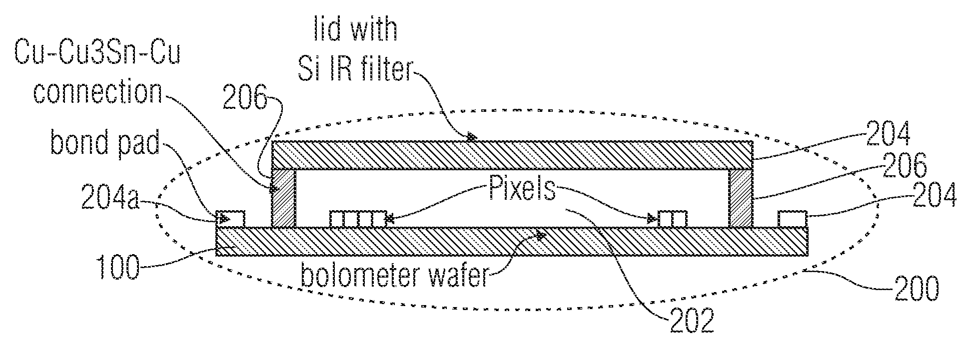
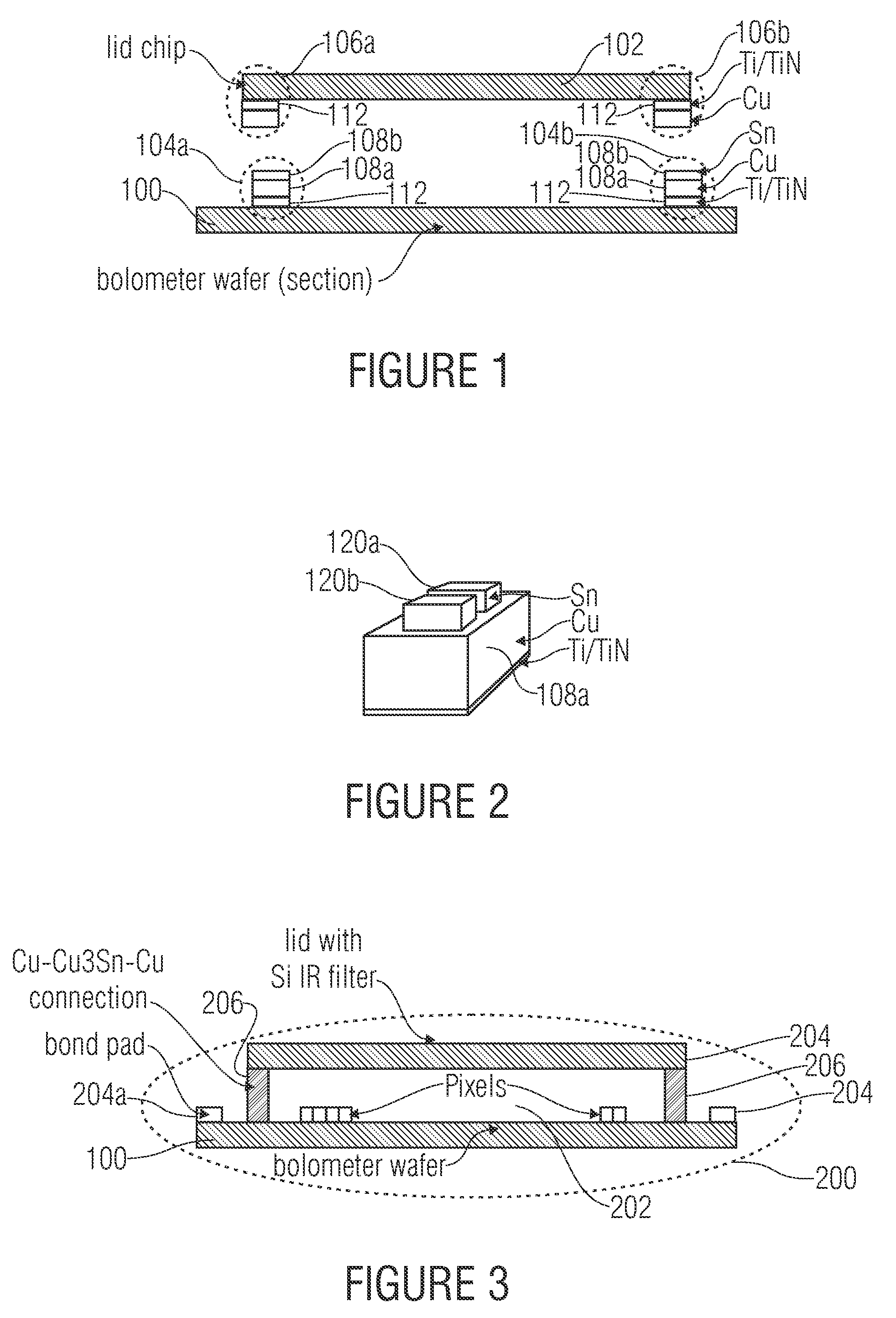
[0041]FIG. 1 shows an example of substrates for creating a package which have been prepared in accordance with the invention.

[0042]FIG. 1 shows a first substrate 100, or a wafer, only a portion of a wafer being shown here, said wafer comprising several of the portions shown in FIG. 1.

[0043]In addition, a second substrate, or a lid chip, 102 is depicted.

[0044]In the sectional view of the wafer 100 and of the lid chip 102, cross-sections of frames 104a and 104b enclosing an electrical circuit on the wafer 100 are also shown on the wafer 100. The inventive complementary counterparts, frames 106a and 106b of the second substrate or lid chip 102, are also depicted in FIG. 1.

[0045]In accordance with the invention, the frame of at least one of the substrates consists of a layer sequence of two metals which together may form an alloy whose the melting point is higher than the melting point of the lower-melting one of the two metals. The frame(s) 104a and / or 104b therefore consists of a firs...


PUM


Abstract

A package including an electrical circuit may be produced in a more efficient manner when on a substrate including a plurality of electrical circuits the circuits are tested for their functionality and when the functional circuits are connected, by means of a frame enclosing the circuit on the surface of the substrate, to a second substrate whose surface area is smaller than that of the first substrate. The substrates are connected, by means of a second frame, which is adapted to the first frame and is located on the surface of the second substrate, such that the first and second frames lie one on top of the other. Subsequently, the functional packaged circuits may be singulated in a technologically simple manner.

Description

BACKGROUND OF THE INVENTION[0001]The present invention relates to packages for electrical circuits, and in particular to such packages, and to a method for manufacturing same, which encapsulate an electrical circuit within a self-contained volume.[0002]Applications in which electrical, optical, micromechanical or other devices may be arranged within a package to ensure their functioning are manifold. For example, infrared sensors for infrared cameras, thermal image cameras or image sensors for night-vision devices are arranged within closed packages for avoiding damage or environmental factors distorting the measurements. In the micromechanical field, this is also true for gyroscopes and electrically adjustable micro-mirrors and other mechanical components such as micromechanical sensors. In cameras for visible light or other sensors, both individual sensors, rows of sensors or entire two-dimensional arrays may be arranged within a package in this context.[0003]With some sensors suc...

Claims


Application Information

Patent Timeline
Patent Type & Authority Applications(United States)
IPC IPC(8): H01L21/50H01L31/02
CPCB81B2201/0278B81C1/00269B81C2203/019G01J5/02G01J5/023G01J5/04H01L27/14683G01J5/046G01J5/0875G01J5/20H01L27/14618H01L27/14649G01J5/045H01L2924/0002H01L2924/00
Inventor VOGT, HOLGERBAUER, JOCHEN
Owner FRAUNHOFER GESELLSCHAFT ZUR FOERDERUNG DER ANGEWANDTEN FORSCHUNG EV
Why Eureka
Try Eureka