Semiconductor device and manufacturing method thereof

Active Publication Date: 2009-04-30
PANNOVA SEMIC
View PDF5 Cites 23 Cited by
  • Summary
  • Abstract
  • Description
  • Claims
  • Application Information

AI Technical Summary

Benefits of technology

[0060]The void width may be smaller than the width of an interconnect formed in the chip region. In this case, the void can be prevented from being filled with an interconnect material such as Cu, whereby the void can be easily formed. As a result, an impact that is generated in a dicing process can be reliably blocked. Moreover, since the void width is small, each void has a small occupied area. Even a plurality of voids can therefore be easily formed between the seal ring and a dicing portion. In other words, the degree of freedom in void formation is improved.
[0061]With the above-desc

Problems solved by technology

This effect, however, is limited only to the passivation film portion.
If the impact generated in the dicing process causes chippings and cracks in a part of the seal ring, moisture, mobile ions, and the like cannot be sufficiently prevented from entering the chip region.
If the semiconductor device in such a state is packaged, debris from the seal ring contacts bonding wires, resulting in a product defect.
However, a low dielectric constant interlayer insulating film generally has low mechanical strength.
The low dielectric constant interlayer insulating film therefore does

Method used


Image

  • Semiconductor device and manufacturing method thereof
  • Semiconductor device and manufacturing method thereof
  • Semiconductor device and manufacturing method thereof

Examples


Example

First Embodiment

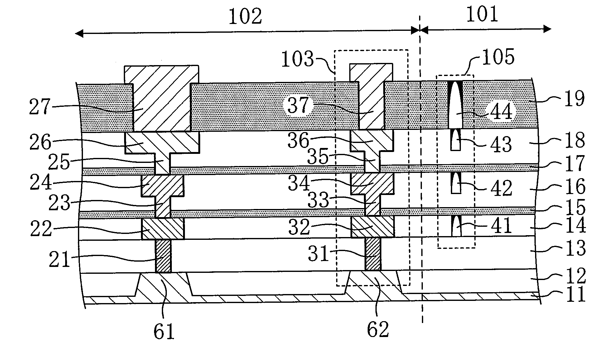
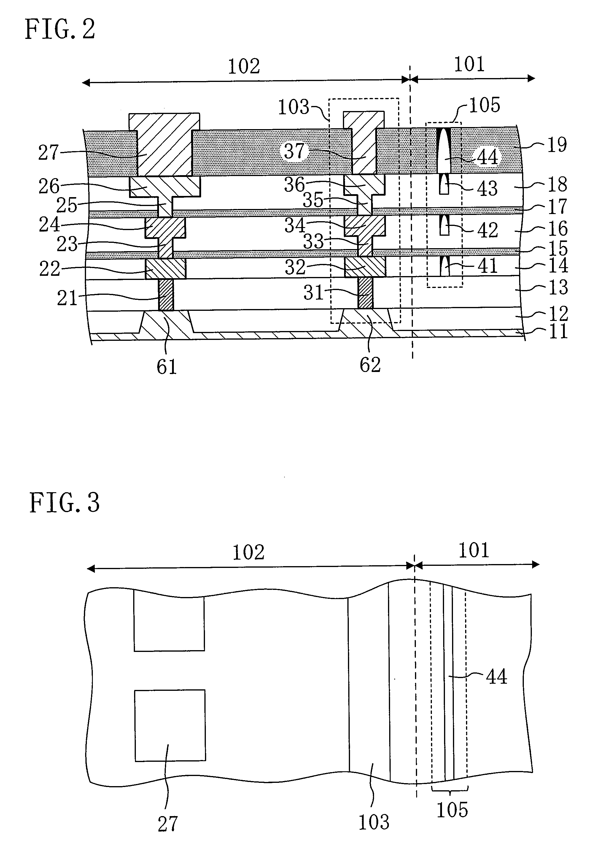
[0088]Hereinafter, a semiconductor device and a manufacturing method thereof according to a first embodiment of the invention will be described with reference to the figures.

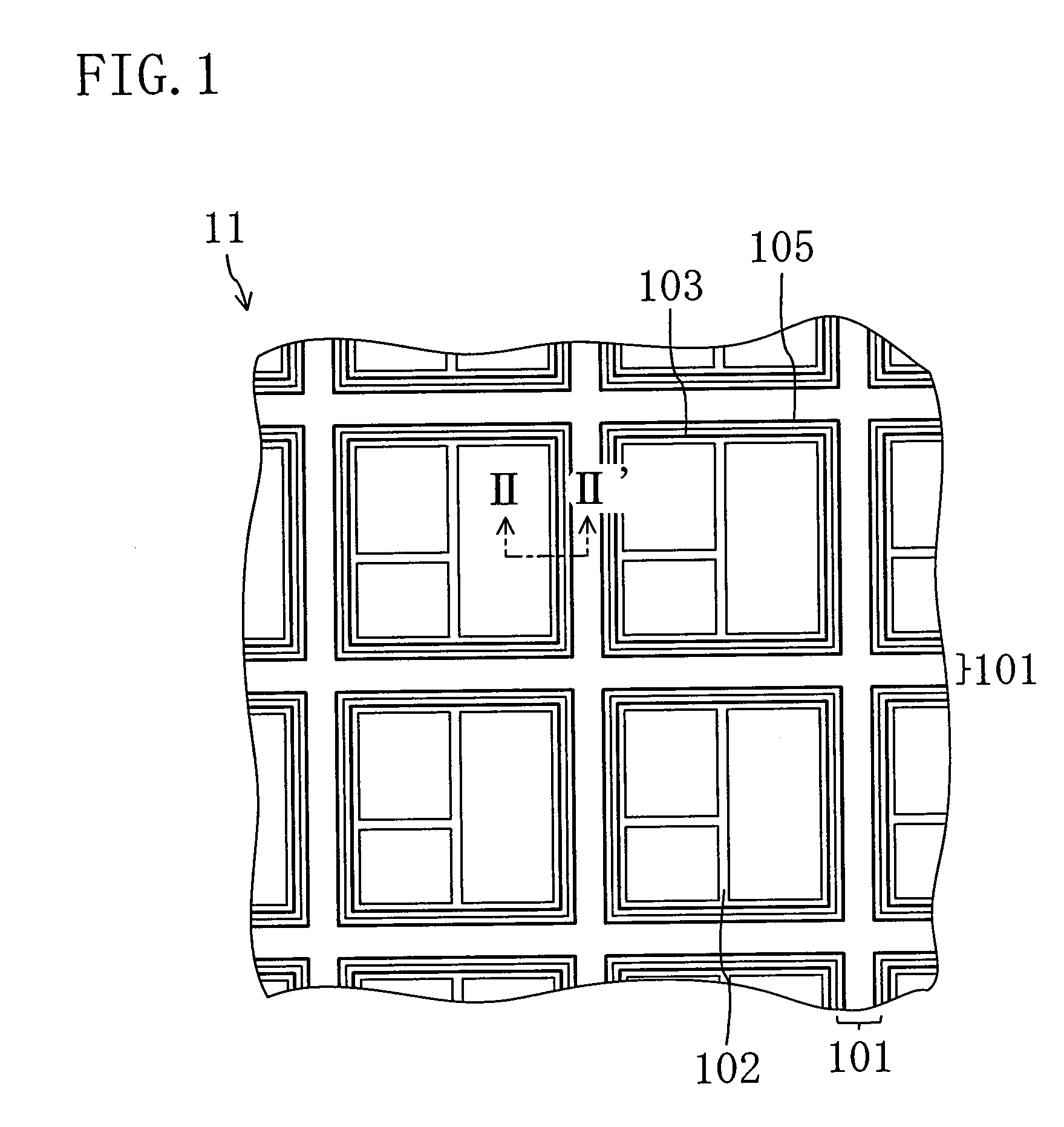
[0089]FIG. 1 is a plan view showing a part of a wafer having semiconductor devices of the first embodiment provided thereon.

[0090]As shown in FIG. 1, a plurality of chip regions 102 that will become semiconductor devices are provided on a wafer that is a semiconductor substrate 11 such as a silicon substrate. An IC (Integrated Circuit) formed by a plurality of elements and having a predetermined function is provided in each chip region 102. The chip regions 102 are separated from each other by a lattice-shaped dicing region 101.

[0091]A semiconductor device (i.e., a semiconductor chip) includes a chip region 102 where an IC formed by a plurality of elements and having a predetermined function is provided, a seal ring 103 provided in the periphery of the chip region 102 so as to surround the chip r...

Example

[0124]Note that the above description applies to second through fourth embodiments described below.

[0125]In the semiconductor device of the first embodiment, a void (41, 42, 43) surrounding a seal interconnect (32, 34, 36) is formed in order to reliably protect an interconnect (22, 24, 26) and a seal interconnect. In order to reduce a dielectric constant between interconnects, a low dielectric constant insulating film is often used for a layer in which an interconnect is formed. In order to provide the effect of the void region 105, it is important to reliably protect a seal interconnect provided at a level where an interconnect is formed. It is more desirable in terms of impact absorption during a dicing process to form a void at a level where an interconnect and a seal interconnect are formed than to form a void only at a level where a via (21, 23, 25) and a seal via (31, 33, 35) are formed (for example, Japanese Laid-Open Patent Publication No. 2006-59976; hereinafter, referred t...

Example

Second Embodiment

[0128]Hereinafter, a semiconductor device and a manufacturing method thereof according to a second embodiment of the invention will be described with reference to the figures.

[0129]FIG. 9 is a plan view showing a part of a wafer having semiconductor devices of the second embodiment provided thereon.

[0130]As shown in FIG. 9, a plurality of chip regions 102 that will become semiconductor devices are provided on a wafer that is a semiconductor substrate 11 such as a silicon substrate. An IC formed by a plurality of elements and having a predetermined function is provided in each chip region 102. The chip regions 102 are separated from each other by a lattice-shaped dicing region 101.

[0131]A semiconductor device (i.e., a semiconductor chip) includes a chip region 102 where an IC formed by a plurality of elements and having a predetermined function is provided, a seal ring 103 provided in the periphery of the chip region 102 so as to surround the chip region 102, and a v...


PUM


Abstract

A semiconductor device includes an element formed on a substrate, at least one insulating film formed on the substrate, and a seal ring formed in the insulating film so as to surround a region where the element is formed and to extend through the insulating film. The semiconductor device further includes a void region including a void and formed in the insulating film in a region located outside the seal ring when viewed from the element.

Description

CROSS REFERENCE TO RELATED APPLICATION[0001]This application claims priority under 35 U.S.C. §119 on Patent Application No. 2007-276464 filed in Japan on Oct. 24, 2007, the entire contents of which are hereby incorporated by reference.BACKGROUND OF THE INVENTION[0002]1. Field of the Invention[0003]The invention relates to a semiconductor device having a seal ring formed so as to surround a chip region and a mechanism for protecting the seal ring, and a manufacturing method of such a semiconductor device.[0004]2. Related Art[0005]Semiconductor devices are generally produced by providing a multiplicity of ICs (Integrated Circuits), each formed by a plurality of elements and having a predetermined function, in a matrix pattern on a semiconductor wafer such as silicon.[0006]A multiplicity of chip regions provided on the wafer are separated from each other by a lattice-shaped dicing region (scribe lines). After a multiplicity of chip regions are formed on a single wafer through a semicon...

Claims


Application Information

Patent Timeline
IPC IPC(8): H01L21/768H01L23/00
CPCH01L21/768H01L21/78H01L23/585H01L2924/0002H01L2924/00
Inventor TSUTSUE, MAKOTO
Owner PANNOVA SEMIC
Why Eureka
Try Eureka