Shifting of a voltage level between different voltage level domains

a voltage level and domain technology, applied in the field of level shifters, can solve problems such as not allowing current to flow

Inactive Publication Date: 2009-04-30
ARM LTD
View PDF3 Cites 17 Cited by
  • Summary
  • Abstract
  • Description
  • Claims
  • Application Information

AI Technical Summary

Benefits of technology

[0037]A further solution to the above problem could be to provide a PMOS transistor arranged as a diode on top of the PMO

Problems solved by technology

This could be a problem if the first voltage domain is lower than the second voltage domain.
Thus, when the device input is tied to the high level of the second voltage domain when the input signal is high, this further switching device does not allow current to flow from the device held at this high level to t

Method used


Image

  • Shifting of a voltage level between different voltage level domains
  • Shifting of a voltage level between different voltage level domains
  • Shifting of a voltage level between different voltage level domains

Examples


Embodiment Construction

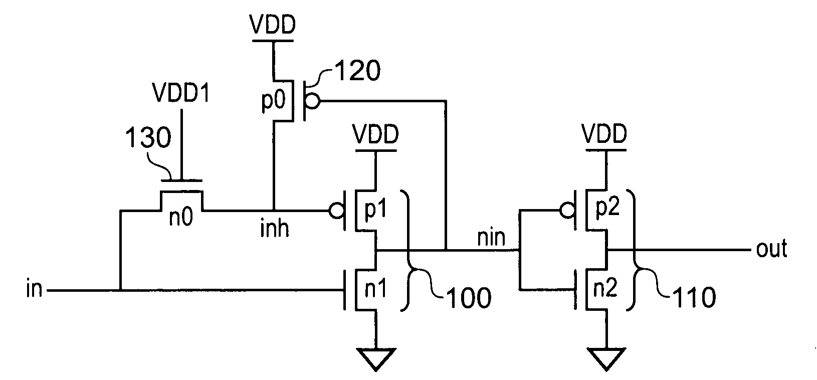
[0050]FIG. 4 shows a voltage level shifter according to an embodiment of the present invention. It comprises an input in for receiving a digital signal in a first voltage domain with a high voltage level of VDDI and an output out for outputting a signal in a second voltage domain with a high voltage level of VDD. The circuit comprises a first inverter 100 comprising a PMOS transistor p1 and an NMOS transistor n1 and a second inverter 110 comprising a PMOS transistor p2 and an NMOS transistor n2. These two inverters act to receive an input signal invert it to produce nin and then invert nin to produce an output signal out. As they are powered by the second voltage domain VDD, the signal they output is in this voltage domain. In addition to these two inverters 100 and 110 the voltage level shifter also comprises two switching devices 120 and 130. Switching device 120 comprises a PMOS transistor connected between the output of the first inverter and its input. This PMOS transistor is p...


PUM


Abstract

A voltage level shifter for receiving a digital signal from a first voltage domain and converting said signal to a digital signal in a second voltage domain is disclosed. The voltage level shifter comprises: an input for receiving said digital signal from said first voltage domain; a device connected to said input of said voltage level shifter for receiving said digital signal from said first voltage domain and for outputting a digital signal in said second voltage domain, said device being powered by said second voltage domain; a first switching device arranged to connect a high level voltage source of said second domain to an input of said device in response to said input digital signal having a high level and to isolate said high level voltage source of said second domain from said input of said device in response to said input digital signal having a low level; and a second switching device arranged between said voltage level shifter input and said input of said device for inhibiting current flow from said high level voltage source of said second domain to said voltage level shifter input in response to a high level signal at said voltage level shifter input and for allowing current flow in both directions between said voltage level shifter input and said input of said device in response to said voltage level shifter input having a low level signal.

Description

BACKGROUND OF THE INVENTION[0001]1. Field of the Invention[0002]The field of the invention relates to level shifters for shifting the voltage level between voltage domains.[0003]2. Description of the Prior Art[0004]Voltage level shifters are known that convert a signal from one voltage domain to a signal suitable for another voltage domain. This allows circuits that work at different voltage levels to interface with each other.[0005]FIG. 1 shows a conventional TTL to CMOS level shifter used for converting the voltages required for TTL to those required for CMOS. This voltage level shifter works very well provided you know the voltages of the input and output supplies. This is because it allows you to tune the size of transistor p3 so that it drops VDD down to VDDI. This is necessary as if VDDI is much less that VDD then when VDDI is input to inverter 10 p1 will not be completely off and therefore there will be leakage through this inverter. If the size of p3 is tuned such that the v...

Claims


Application Information

Patent Timeline
IPC IPC(8): H03L5/00
CPCH03K19/018521H03K19/0016
Inventor SHIFFER, II, JAMES DAVID
Owner ARM LTD
Why Eureka
Try Eureka