Method and system for performing electrostatic chuck clamping in track lithography tools

a technology of lithography tool and chuck, applied in the direction of electrical equipment, semiconductor/solid-state device manufacturing, basic electric elements, etc., can solve the problems of significant reduction of chucking pressure, loss of yield, degradation of device characteristics and reliability, etc., and achieve the effect of improving chucking pressur

Inactive Publication Date: 2009-04-30
SOKUDO CO LTD
View PDF9 Cites 99 Cited by
  • Summary
  • Abstract
  • Description
  • Claims
  • Application Information

AI Technical Summary

Benefits of technology

[0013]Depending upon the embodiment, many benefits can be achieved, particularly for achieve enhanced chucking pressure for clamping semiconductor wafer on a bipolar electrostatic chuck in ambient environment where the pressure can be as high as on...

Problems solved by technology

However, one potential problem is that if a substrate wafer is loaded directly onto the upper surface of a conventional electrostatic chuck during substrate processing, the chuck surface can abrade the material present on the backside of the substrate wafer, resulting in the introduction of particulate contaminants to the process environment.
The particulate contaminants can adhere to the backside of another substrate wafer and be carried to other process environment or cause defects in the circuitry fabricated upon the substrate wafer.
As the semiconductor device geometry has become smaller with each generation of ICs, these particulate contaminants can cause a loss in...

Method used


Image

  • Method and system for performing electrostatic chuck clamping in track lithography tools
  • Method and system for performing electrostatic chuck clamping in track lithography tools
  • Method and system for performing electrostatic chuck clamping in track lithography tools

Examples


Embodiment Construction

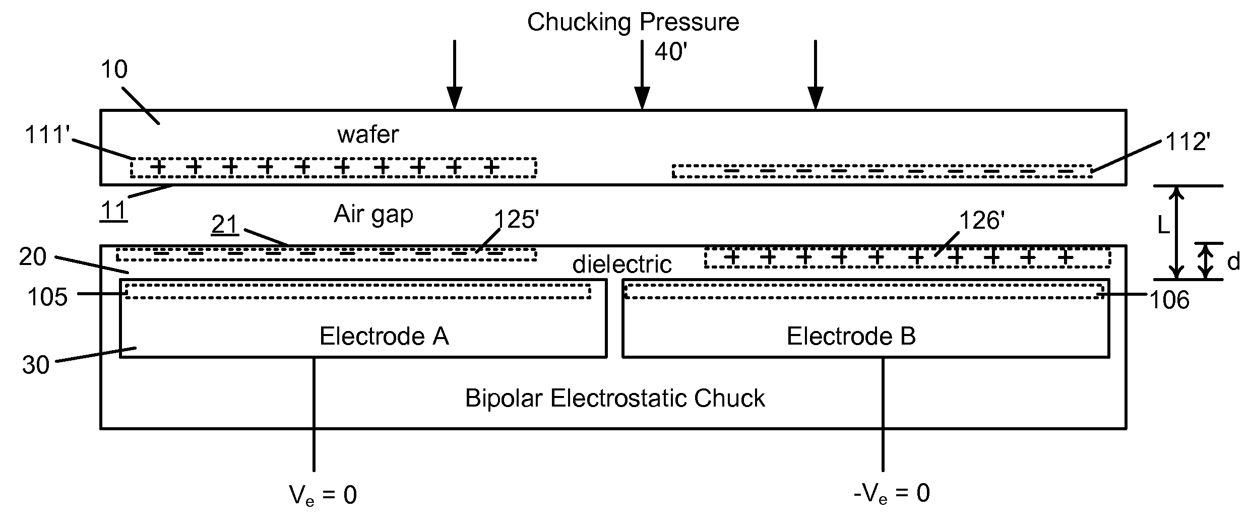
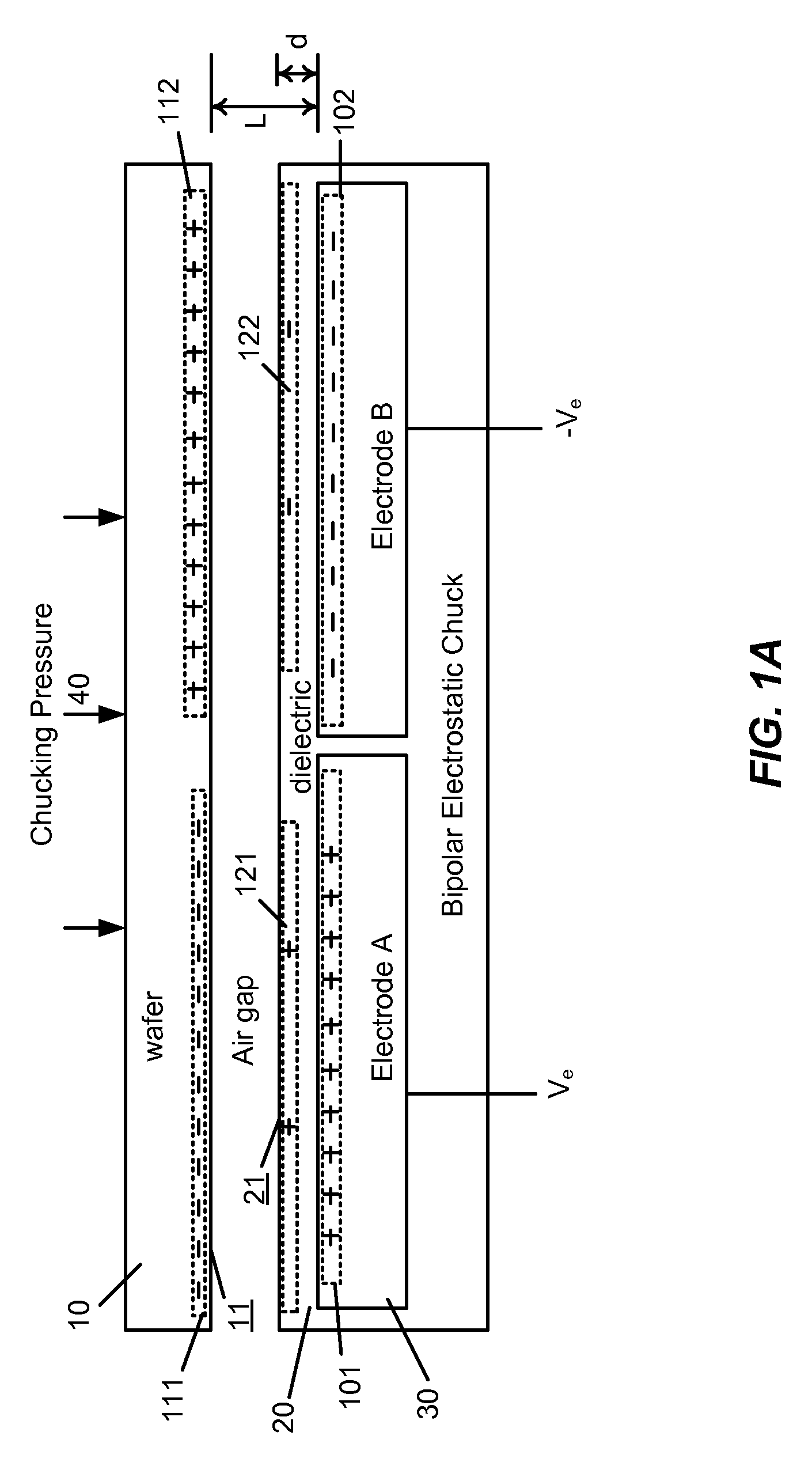
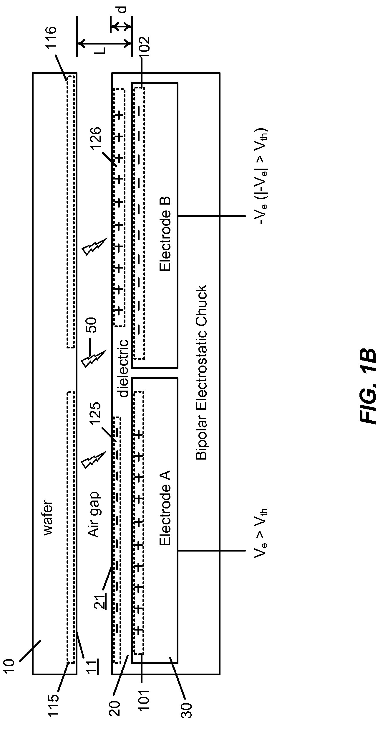
[0022]FIGS. 1A-1C schematically show exemplary electrostatic chucking sequences used for wafer handling in a track lithography tool according to an embodiment of the present invention. As shown in FIG. 1A, a bipolar electrostatic chuck 20 is provided. The bipolar electrostatic chuck 20 includes a dielectric plate and two electrodes 30, e.g., Electrode A and Electrode B, being embedded therein. A semiconductor wafer 10 can be disposed at a predetermined distance above an upper surface 21 of the dielectric plate of the bipolar electrostatic chuck 20. In FIG. 1A, d is denoted as a thickness of the dielectric plate, i.e., a distance between the upper surface 21 of the dielectric plate and each of the two electrodes 30. L is denoted as a distance between a lower surface 11 of the semiconductor wafer 10 and each of the two electrodes 30. Thus, the difference (L−d) is the predetermined distance at which the wafer 10 is disposed above the surface 21, representing a gap-distance between the ...


PUM


Abstract

A method of clamping/declamping a semiconductor wafer on an electrostatic chuck in ambient air includes disposing the semiconductor wafer at a predetermined distance above a dielectric surface of the electrostatic chuck having one or more electrodes and applying a first voltage greater than a predetermined threshold to the one or more electrodes of the electrostatic chuck for a first time period. The method includes reducing the first voltage to a second voltage substantially equal to a self bias potential of the semiconductor wafer after the first time period. The method includes maintaining the second voltage for a second time period and adjusting the second voltage to a third voltage characterized by a polarity opposite to that of the first voltage and a magnitude smaller than the predetermined threshold. The method includes reducing the third voltage to a fourth voltage substantially equal to the second voltage after a third time period.

Description

BACKGROUND OF THE INVENTION[0001]The present invention relates generally to the field of substrate processing equipment. More particularly, the present invention relates to a method and apparatus for performing electrostatic chucking of a semiconductor substrate wafer. Merely by way of example, the method and apparatus of the present invention are applied to clamp and declamp a semiconductor wafer on an electrostatic chuck for ambient thermal processing in a track lithography tool. The method and apparatus can be applied to other processing devices for semiconductor processing equipments utilized in other processing chambers.[0002]Modem integrated circuits contain millions of individual elements that are formed by patterning the materials, such as silicon, metal and dielectric layers, that make up the integrated circuit to sizes that are small fractions of a micrometer. The technique used throughout the industry for forming such patterns is photolithography. A typical photolithograp...

Claims


Application Information

Patent Timeline
IPC IPC(8): H01L21/683
CPCH01L21/6831
Inventor HERCHEN, HARALDVELLORE, KIMLUE, BRIAN C.
Owner SOKUDO CO LTD
Why Eureka
Try Eureka