Graphene sheet and method of preparing the same

a graphene sheet and graphene technology, applied in the field of graphene sheets, can solve the problems of high cost of carbon nanotubes, difficulty in separating single-walled carbon nanotubes, and the inability to economically and reproducibly prepare a large-scale graphene sh

Active Publication Date: 2009-04-30
SAMSUNG ELECTRONICS CO LTD
View PDF5 Cites 339 Cited by
  • Summary
  • Abstract
  • Description
  • Claims
  • Application Information

AI Technical Summary

Benefits of technology

[0011]Disclosed is an economical method of preparing a

Problems solved by technology

However carbon nanotubes are expensive due to low yields during synthesis and purification processes.
However, separating single wall carbon nanotubes is problematic.
However, although graphene sheets have these advantageous characteristics, a method of economically and reproducibly preparing a large-sized graphene sheet has not yet been developed.
In this case, the separated gra

Method used


Image

  • Graphene sheet and method of preparing the same
  • Graphene sheet and method of preparing the same
  • Graphene sheet and method of preparing the same

Examples


example 1

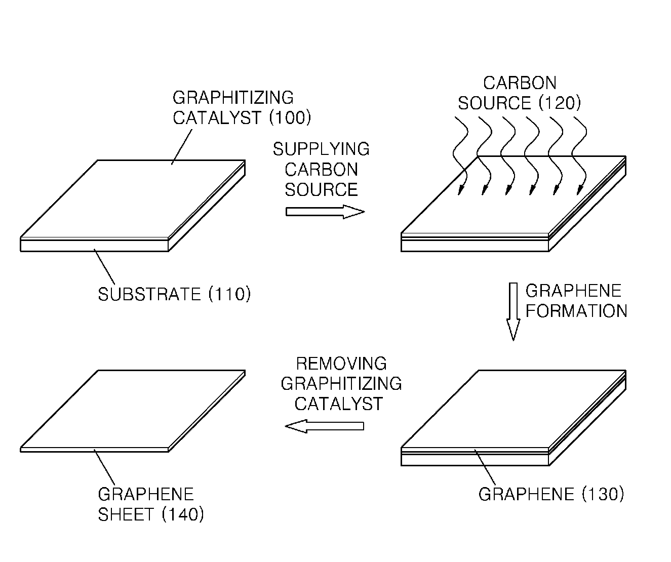
[0074]A graphitizing catalyst film was formed by depositing Ni on a 1.2 cm×1.5 cm silicon substrate on which 100 nm of SiO2 was coated by sputtering to form a Ni thin film with a thickness of 100 nm. The silicon substrate on which the SiO2 and Ni thin film were formed was disposed in a chamber, and the substrate heat-treated at 400° C. for 20 minutes using a halogen lamp as a heat source while acetylene gas was added to the chamber at a constant rate of 200 sccm to form graphene on the graphitizing catalyst.

[0075]Then, a 7 layered graphene sheet having a size of 1.2 cm×1.5 cm was formed by removing the heat source and naturally cooling the interior of the chamber to grow graphene in a uniform arrangement.

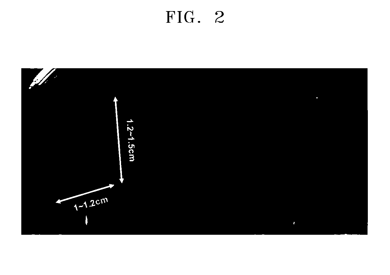
[0076]Then, the substrate including the graphene sheet was immersed in 0.1 M HCI for 24 hours to remove the Ni thin film. The graphene sheet separated from the substrate during the immersion. FIG. 2 is a photographic image of the graphene sheet prepared according to Example 1.

[0077]...

example 2

[0079]A 16 layered graphene sheet having a size of 1.2 cm×1.5 cm was prepared in the same manner as in Example 1, except that the heat-treatment was performed at 500° C. instead of 400° C.

[0080]Then, the substrate including the graphene sheet was immersed in 0.1 M HCI for 24 hours to remove the Ni thin film. The graphene sheet separated from the substrate during the immersion.

[0081]FIG. 3 is a graph illustrating a Raman spectrum of the graphene sheet. Referring to FIG. 3, the formation of graphene can be identified by the G′ peak shown at 1594 cm−1.

[0082]FIG. 5 is a SEM image of the graphene sheet formed in Example 2. Referring to FIG. 5, it can be seen that a uniform graphene sheet was formed because features are not observed in the SEM image.

example 3

[0083]A 32 layered graphene sheet having a size of 1.2 cm×1.5 cm was prepared in the same manner as in Example 1, except that the heat-treatment was performed at 600° C. instead of 400° C.

[0084]Then, the substrate including the graphene sheet was immersed in 0.1 M HCI for 24 hours to remove the Ni thin film. The graphene sheet separated during the immersion.

[0085]FIG. 3 is a graph illustrating a Raman spectrum of the graphene sheet. Referring to FIG. 3, the formation of graphene can be identified by the G′ peak shown at 1594 cm−1.


PUM

PropertyMeasurementUnit
Temperatureaaaaaaaaaa
Timeaaaaaaaaaa

Abstract

An economical method of preparing a large-sized graphene sheet having a desired thickness includes forming a film, the film comprising a graphitizing catalyst; heat-treating a gaseous carbon source in the presence of the graphitizing catalyst to form graphene; and cooling the graphene to form a graphene sheet. A graphene sheet prepared according to the disclosed method is also described.

Description

[0001]This application claims priority to of Korean Patent Application No. 10-2007-0108860, filed on Oct. 29, 2007 and Korean Patent Application No. 10-2008-0023457, filed on Mar. 13, 2008, and all the benefits accruing therefrom under 35 U.S.C. §119, the contents of which in their entirety are herein incorporated by reference.BACKGROUND OF THE INVENTION[0002]1. Field of the Invention[0003]This disclosure relates to a graphene sheet and a method of preparing the same.[0004]2. Description of the Related Art[0005]Generally, graphite is a stack of two-dimensional graphene sheets formed from a planar array of carbon atoms bonded into hexagonal structures. Recently, testing of graphene sheets has revealed beneficial properties of single or multiple-layered graphene sheets.[0006]One beneficial property of graphene is that electrons flow in an entirely unhindered fashion in a graphene sheet, which is to say that the electrons flow at the velocity of light in a vacuum. In addition, graphene...

Claims


Application Information

Patent Timeline
IPC IPC(8): C01B31/04B32B9/00H01B1/04
CPCB82Y30/00B82Y40/00C01B31/0453C01B2204/02C01B2204/04Y10T428/261C23C16/01C23C16/0281C23C16/26C23C16/56Y02E60/324C01B2204/32C01B32/186C01B32/194Y02E60/32
Inventor CHOI, JAE-YOUNGSHIN, HYEON-JINYOON, SEON-MI
Owner SAMSUNG ELECTRONICS CO LTD
Why Eureka
Try Eureka