Film formation apparatus for semiconductor process

a technology of film formation apparatus and semiconductor device, which is applied in the direction of coating, chemical vapor deposition coating, metallic material coating process, etc., can solve the problems of reducing the yield of semiconductor device to be fabricated, deteriorating some components of processing apparatus, and affecting the uniformity of cleaning process, so as to achieve uniform cleaning process

Inactive Publication Date: 2009-05-07
TOKYO ELECTRON LTD
View PDF11 Cites 16 Cited by
  • Summary
  • Abstract
  • Description
  • Claims
  • Application Information

AI Technical Summary

Benefits of technology

[0009]An object of the present invention is to provide a film formation apparatus for a semiconductor process, which allows a cleaning process to be uniformly and effectively performed overall inside a reaction tube. Another object of the present invention is to provide a film formation apparatus for a semiconductor process, which can prevent a gas nozzle of a cleaning gas from being deteriorated.

Problems solved by technology

If the film formation process is continued while by-product films are present on the inner surface of the reaction tube and so forth, a stress is generated and causes peeling of some of the by-product films and the quartz of the reaction tube and so forth due to a difference in coefficient of thermal expansion between the quartz and by-product films.
Consequently, particles are generated, and may decrease the yield of semiconductor devices to be fabricated and / or deteriorate some components of the processing apparatus.
However, as described later, the present inventors have found that conventional film formation apparatuses of this kind entail problems in relation to a cleaning process performed inside a reaction tube such that the cleaning process may be less effective on the upper side of the reaction tube or a gas nozzle of a cleaning gas is easily deteriorated.

Method used


Image

  • Film formation apparatus for semiconductor process
  • Film formation apparatus for semiconductor process
  • Film formation apparatus for semiconductor process

Examples


Embodiment Construction

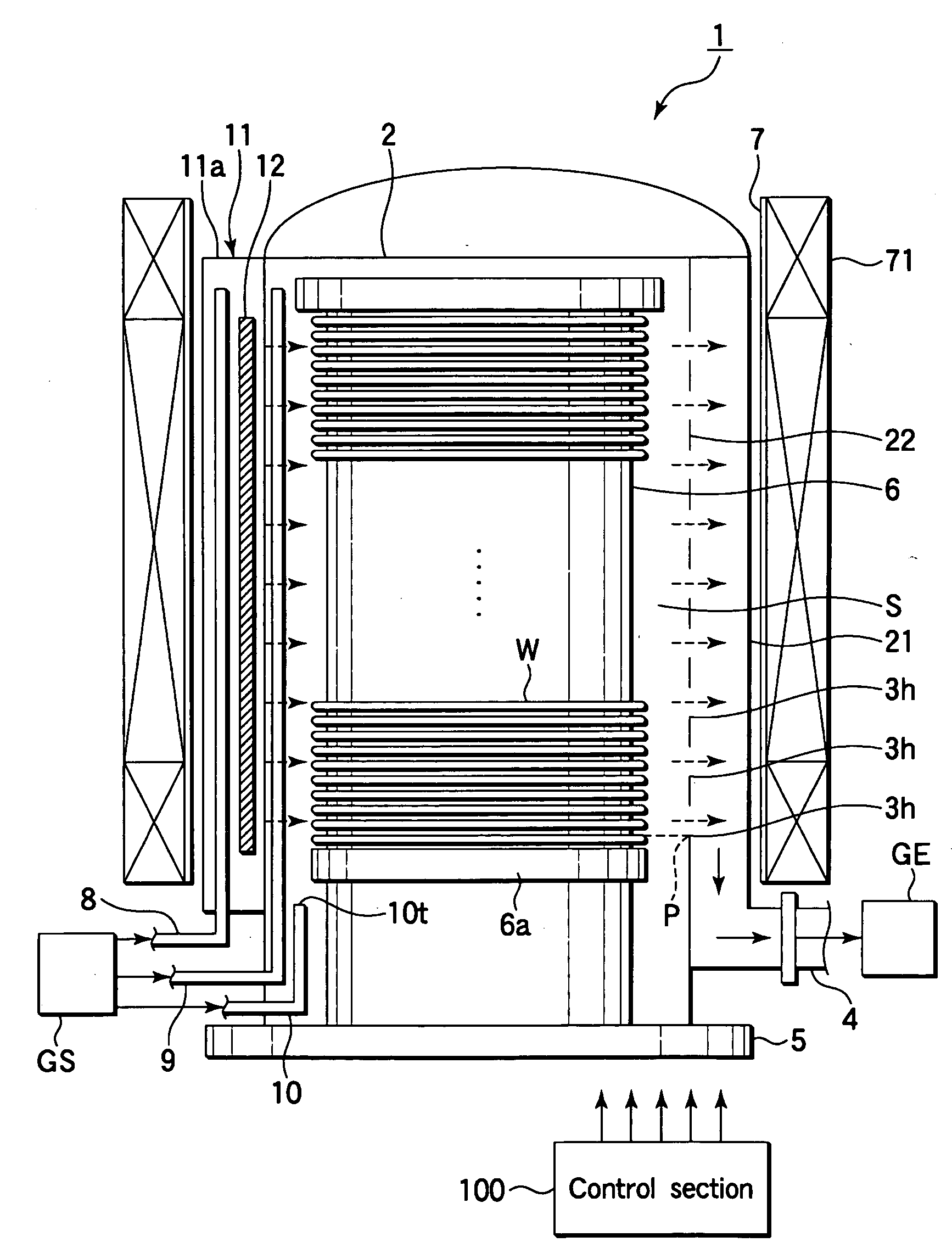
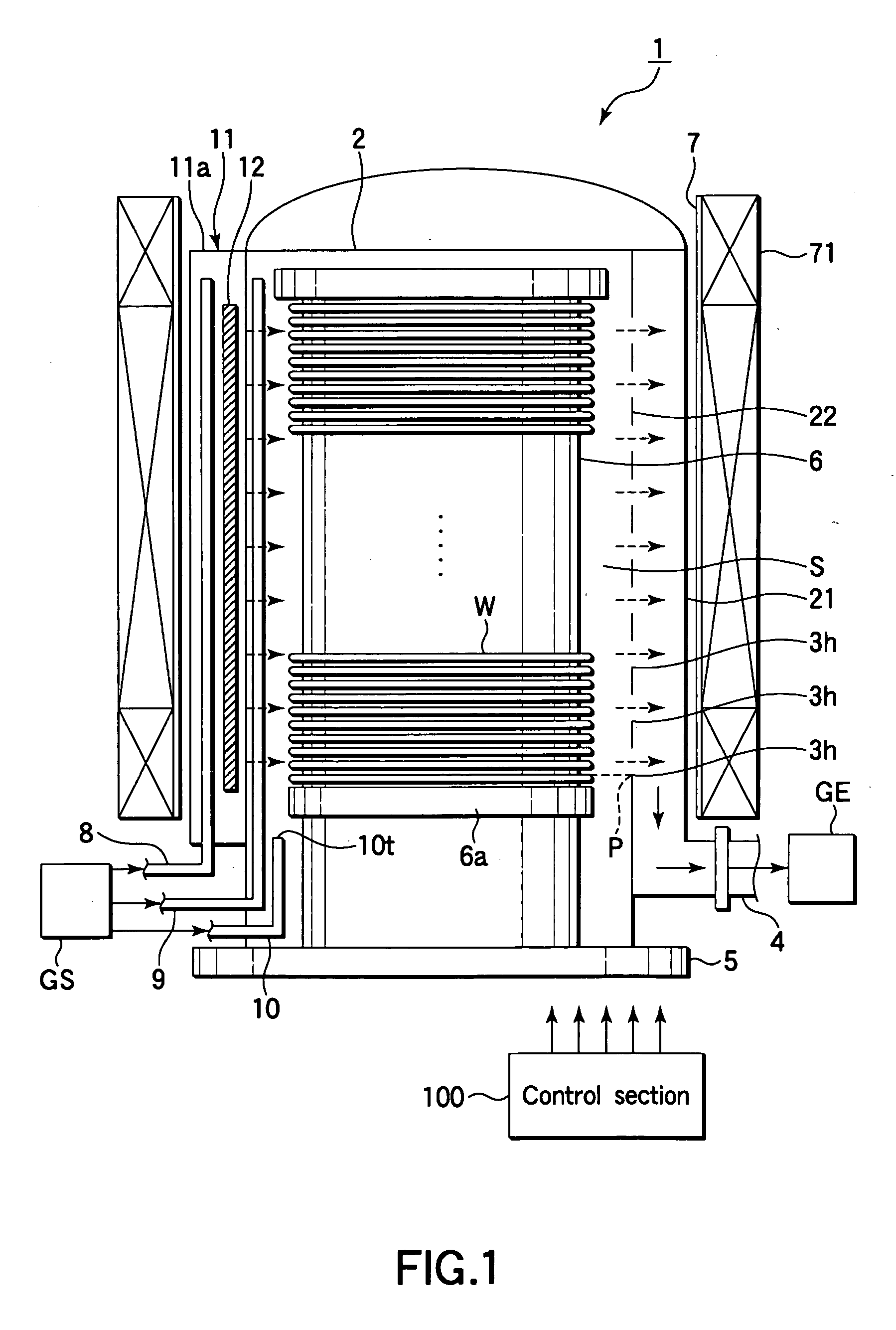
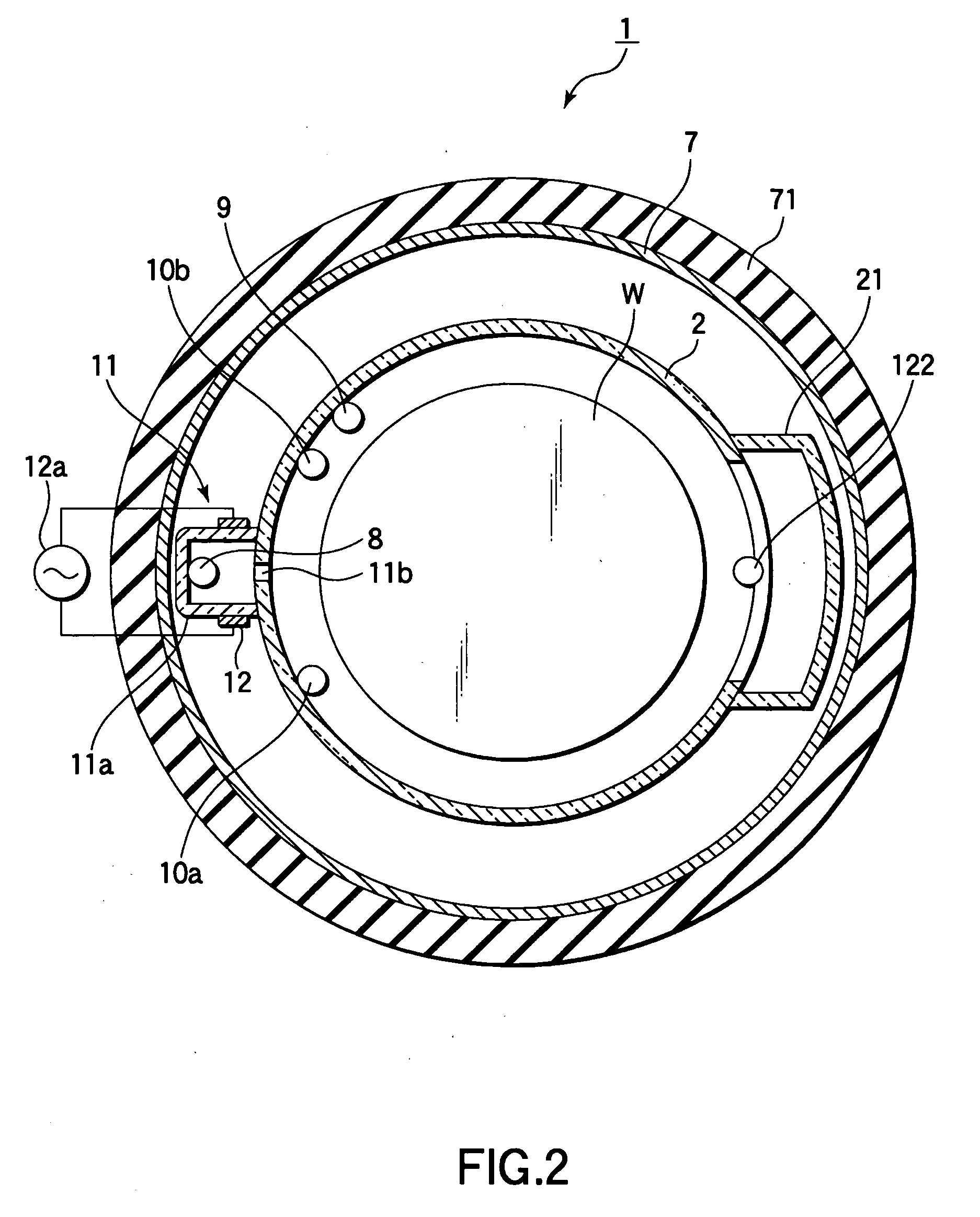
[0019]In the process of developing the present invention, the inventors studied problems entailed by conventional film formation apparatuses for a semiconductor process in relation to a cleaning process inside a reaction chamber. As a result, the inventors have arrived at the findings given below.

[0020]Specifically, film formation apparatuses of this kind include a type in which a reaction tube is provided with a cleaning gas nozzle disposed on a lower side for supplying a cleaning gas and an exhaust port formed on a lower side for exhausting gas from inside the reaction tube. In such a film formation apparatus, the cleaning gas supplied from the cleaning gas nozzle may insufficiently reach the upper side of the reaction tube. If supply of the cleaning gas is insufficient on the upper side of the reaction tube, by-product films are left on the upper side, and thus the cleaning process becomes less effective for the film formation apparatus.

[0021]On the other hand, the cleaning gas n...


PUM

PropertyMeasurementUnit
frequencyaaaaaaaaaa
frequencyaaaaaaaaaa
diameteraaaaaaaaaa

Abstract

A film formation apparatus for a semiconductor process includes a support member having a plurality of support levels configured to support target substrates inside a reaction chamber; a film formation gas supply system configured to supply a film formation gas into the reaction chamber and including a gas distribution nozzle; a cleaning gas supply system configured to supply a cleaning gas for etching a by-product film deposited inside the reaction chamber; and an exhaust system configured to exhaust gas from inside the reaction chamber. The cleaning gas supply system includes a gas nozzle disposed near a bottom of the reaction chamber and having a gas supply port at its top directed upward, and the gas supply port is located below the lowermost one of the support levels of the support member.

Description

BACKGROUND OF THE INVENTION[0001]1. Field of the Invention[0002]The present invention relates to a film formation apparatus for a semiconductor process for forming a thin film, such as a silicon nitride film, on a target substrate, such as a semiconductor wafer. The term “semiconductor process” used herein includes various kinds of processes which are performed to manufacture a semiconductor device or a structure having wiring layers, electrodes, and the like to be connected to a semiconductor device, on a target substrate, such as a semiconductor wafer or a glass substrate used for an FPD (Flat Panel Display), e.g., an LCD (Liquid Crystal Display), by forming semiconductor layers, insulating layers, and conductive layers in predetermined patterns on the target substrate.[0003]2. Description of the Related Art[0004]In manufacturing semiconductor devices, a process, such as CVD (Chemical Vapor Deposition), is performed to form a thin film, such as a silicon nitride film or silicon ox...

Claims


Application Information

Patent Timeline
Patent Type & Authority Applications(United States)
IPC IPC(8): C23C16/00
CPCC23C16/345H01L21/3185C23C16/45525C23C16/4405H01L21/0217H01L21/205
Inventor NODERA, NOBUTAKESATO, JUNYAMAMOTO, KAZUYAHASEBE, KAZUHIDE
Owner TOKYO ELECTRON LTD
Why Eureka
Try Eureka