Plasma processing apparatus for vapor phase etching and cleaning

a technology of vapor phase etching and processing apparatus, which is applied in the direction of electrical apparatus, basic electric elements, electric discharge tubes, etc., can solve the problems of difficult control of cleaning solution amount and cleaning uniformity, damage to plasma depending on processes, and difficulty in controlling the amount of cleaning solution

Inactive Publication Date: 2015-03-05
GENERAL CO LTD
View PDF0 Cites 6 Cited by
  • Summary
  • Abstract
  • Description
  • Claims
  • Application Information

AI Technical Summary

Benefits of technology

[0024]The plasma apparatus for vapor etching and cleaning may clean the substrate to be processed without any plasma damage. Further, it has advantages that there does not occur any residual product and the selectivity is high. Furthermore, the surface of the substrate to be processed may be uniformly cleaned by providing the substrate to be process with the gasified gas for the vapor phase cleaning. The temperature of the gasified gas may be controlled using the heater disposed in the has distribution baffle to inject the gasified gas. Furthermore, the substrate to be processed may be cleaned even in the micro-pattern processing process since there is no plasma damage.

Problems solved by technology

Accordingly, as the device design becomes smaller and smaller, there occurs a problem in that the pattern is damaged depending on processes.
However, the wet process also has a drawback that there occurs a huge amount of waste water and it is difficult to control the amount of cleaning solution and cleaning uniformity.
Further, in case of anisotropic etching, the pattern after cleaning may be larger or smaller compared with the intended design, so that it becomes difficult to process fine patterns.
Therefore, some problems are emerging, which did not occur in the conventional semiconductor process or were not important.
Among them, a typical problem caused by plasma is plasma damage.
The plasma damage affects, in property and reliability, devices including transistor in all processes in which the wafer surface is exposed as the semiconductor device becomes miniaturized.
Film damage by the electric charge caused by plasma normally occurs in the etching process.
The plasma damage is a problem occurring in the dry etching process or the wet etching process, thereby requiring efforts to solve it.

Method used


Image

  • Plasma processing apparatus for vapor phase etching and cleaning
  • Plasma processing apparatus for vapor phase etching and cleaning
  • Plasma processing apparatus for vapor phase etching and cleaning

Examples


Embodiment Construction

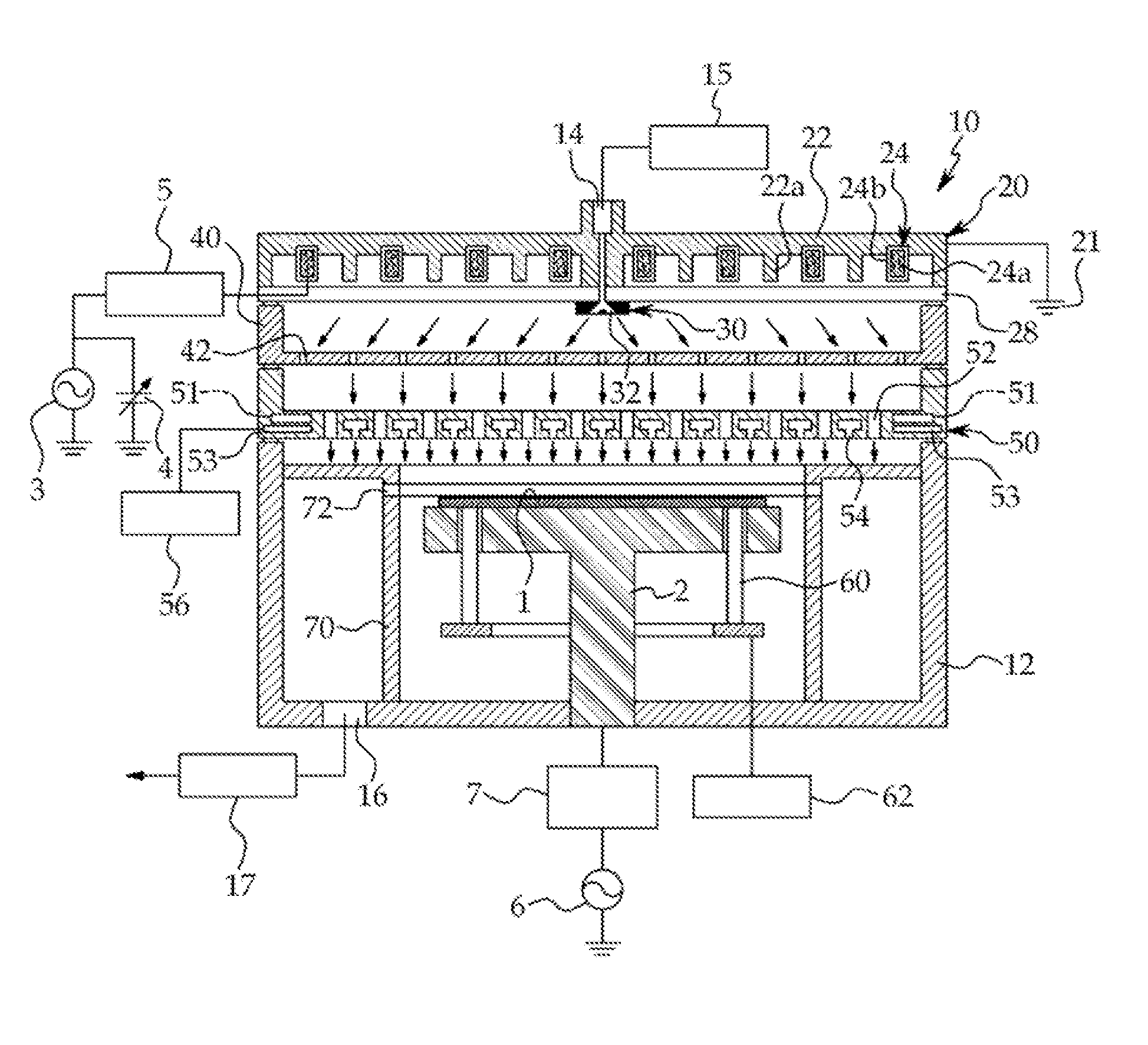
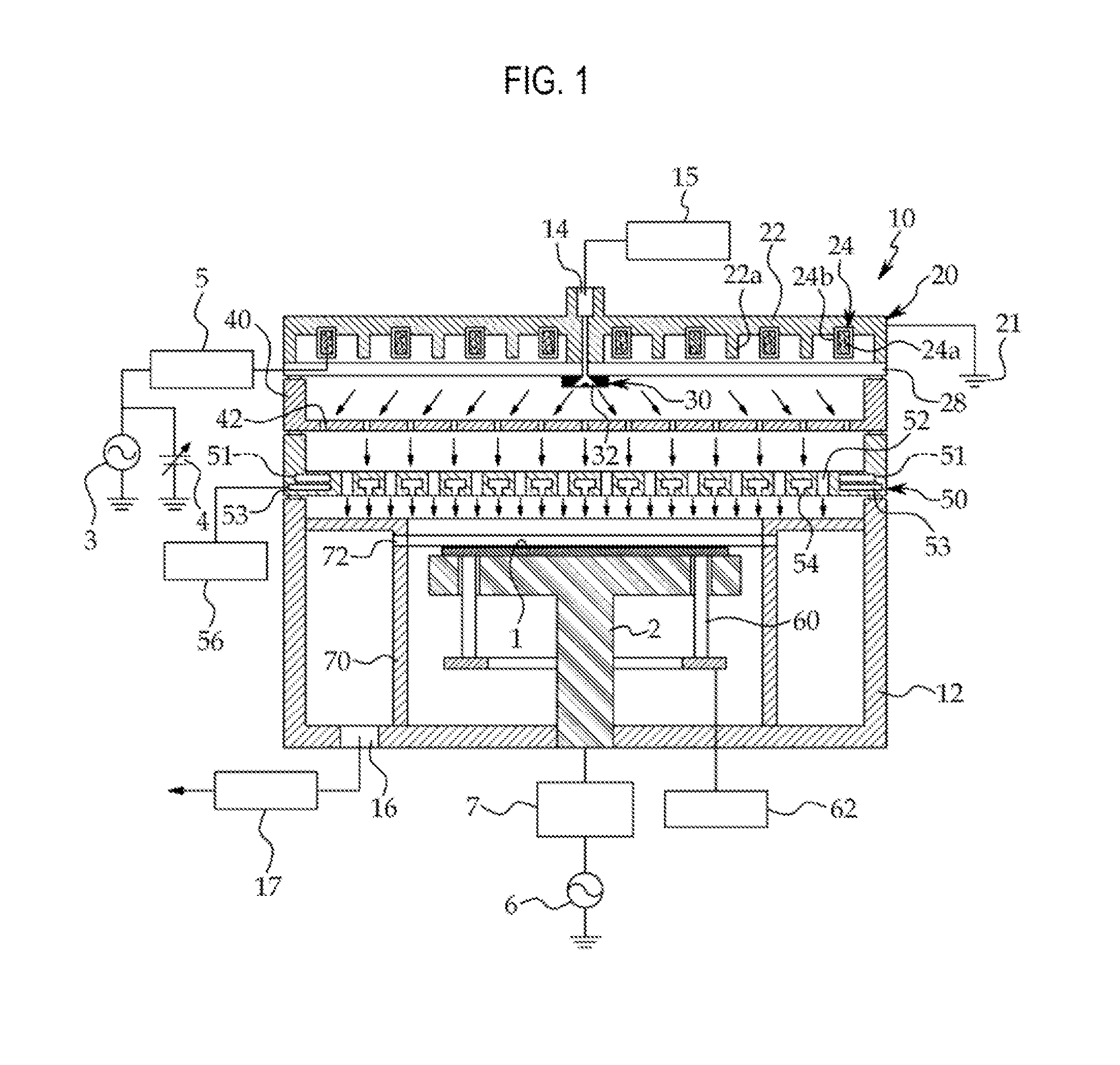
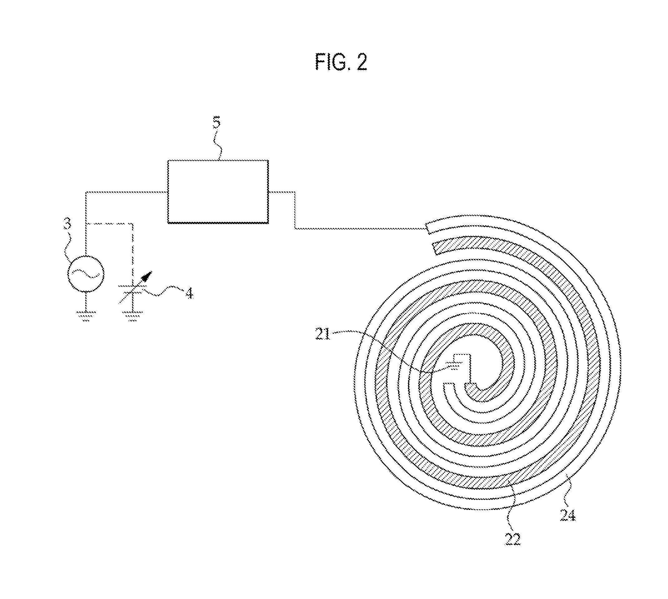
[0033]Hereinafter, embodiments of the present invention will be described in detail with reference to the accompanying drawings so that the present invention can be readily understood by those stilled in the art. The embodiments of the present invention may be modified in a variety of forms and the scope of the present invention should not be construed to be limited to the embodiments described below. The embodiments of the present invention are provided to fully describe them for those skilled in the art. Accordingly, shapes of elements and the like in the drawings may be exaggerated to emphasize a clear explanation. It is noted that the same parts may be identified by the same reference numeral in each drawing. Also, description of well-known functions and constructions are omitted for clarify and conciseness.

[0034]FIG. 1 is a view illustrating a plasma processing apparatus in accordance with a preferred embodiment of the present invention and FIG. 2 is a view illustrating a simpl...


PUM

PropertyMeasurementUnit
areaaaaaaaaaaa
temperatureaaaaaaaaaa
poweraaaaaaaaaa

Abstract

A plasma apparatus for vapor phase etching and cleaning, includes a reactor body configured to process a substrate; a direct plasma generation area in the reactor body, into which a process gas is introduced and in which plasma is directly induced to disassociate the process gas; a substrate processing area in the reactor body in which the substrate is processed by reactive species produced by reacting the disassociated process gas introduced from the direct plasma generation area with a vaporised gas introduced from the outside of the reactor body; a plasma induction assembly configured to induce plasma in the direct plasma generation area; and a gas distribution baffle, disposed between the direct plasma generation area and the substrate processing area, having a plurality of through holes through which the disassociated process gas is introduced from the direct plasma generation area to the substrate processing area.

Description

CROSS-REFERENCE TO RELATED APPLICATIONS[0001]The present application claims priority of Korean Patent Application No. 10-2013-0102625, filed on Aug. 28, 2013, which is incorporated herein by reference in its entirety.FIELD OF THE INVENTION[0002]The present invention relates to a plasma processing apparatus for vapor phase etching and cleaning, and more specifically, to a plasma processing apparatus for vapor phase etching and cleaning, capable of selectively cleaning a surface of a substrate to be processed by causing a direct reaction between a thin film of the surface of the substrate to be processed and high reactive atoms or molecules.BACKGROUND OF THE INVENTION[0003]A semiconductor device is an active electronic device having functions of storing, amplifying and switching electrical signals, which is a core part that guides high added values of system and service industries and leads digital information era based on high integration, high performance and low power consumption.[...

Claims


Application Information

Patent Timeline
Patent Type & Authority Applications(United States)
IPC IPC(8): H01J37/32
CPCH01J37/32633H01J37/3244H01J37/32577H01J2237/335H01J2237/327H01J2237/334H01J37/32522H01J37/32091H01J37/32357H01J37/32449H01J37/32541H01J37/32568H01L21/3065
Inventor KIM, GYOO DONGKANG, SUNG YONGSHIN, WOO GON
Owner GENERAL CO LTD
Why Eureka
Try Eureka