
Module having built-in electronic component and method for manufacturing such module

a technology of electronic components and modules, applied in the direction of electrical apparatus, semiconductor devices, semiconductor/solid-state device details, etc., can solve the problems of deteriorating the reliability of the electric connection of the inner via, difficult to fill the space fully to the bottom with conductive resin composition, and difficult to arrange the inner vias in the vicinity of the semiconductor chip, etc., to achieve the effect of improving the reliability of the electric connection

Inactive Publication Date: 2009-05-07
PANASONIC CORP
View PDF8 Cites 17 Cited by
  • Summary
  • Abstract
  • Description
  • Claims
  • Application Information

AI Technical Summary

Benefits of technology

"The present invention provides an electronic component embedded module that allows for the arrangement of inner vias in the vicinity of an electronic component and improves the reliability of electrical connection of the inner vias. The module includes an electrical insulating substrate with first and second electrical insulating layers, and first and second wiring patterns. The first electronic component is embedded in the second electrical insulating layer and connected electrically to the first wiring pattern through first inner vias. The second electronic component is embedded in the third electrical insulating layer and connected electrically to the second wiring pattern through second inner vias. The first and second inner vias are arranged continuously. The present invention also provides a method for manufacturing the electronic component embedded module. The technical effects of the invention include improved reliability of electrical connection and reduced likelihood of failure of the electronic component."

Problems solved by technology

However, in an electronic component embedded module obtained by the above-described manufacturing method, the sealing agent injected into the space between the semiconductor chip and the wiring pattern will spew out from the edge face of the semiconductor ship, resulting in difficulty in arranging inner vias in the vicinity of the semiconductor chip.
As a result, in the step of filling the space with a conductive resin composition, it is difficult to fill the space fully to the bottom with the conductive resin composition.
Moreover, the chips formed during the blind via processing make a residue, and the residue may adhere onto the wiring pattern for inner via connection, which may degrade the reliability of the electric connection of the inner vias.
As a result, filling with the conductive resin composition may be difficult, and there may be a risk that a clearance is formed between the conductive resin composition and a land for connecting inner vias.
This may degrade further the reliability of the electric connection of the inner vias.
On the other hand, when the inner via diameter is increased to 400 μm or more for the purpose of lowering the aspect ratio, the wiring pattern density is lowered and thus the high-density mounting will be difficult.
And thus, when a crack occurs between the back face and the sealing resin, the crack may spread up to the interface between the sealing resin and the inner vias.
Similarly in this case, the reliability of the electric connection of the inner vias may deteriorate.

Method used


Image

  • Module having built-in electronic component and method for manufacturing such module
  • Module having built-in electronic component and method for manufacturing such module
  • Module having built-in electronic component and method for manufacturing such module

Examples


first embodiment

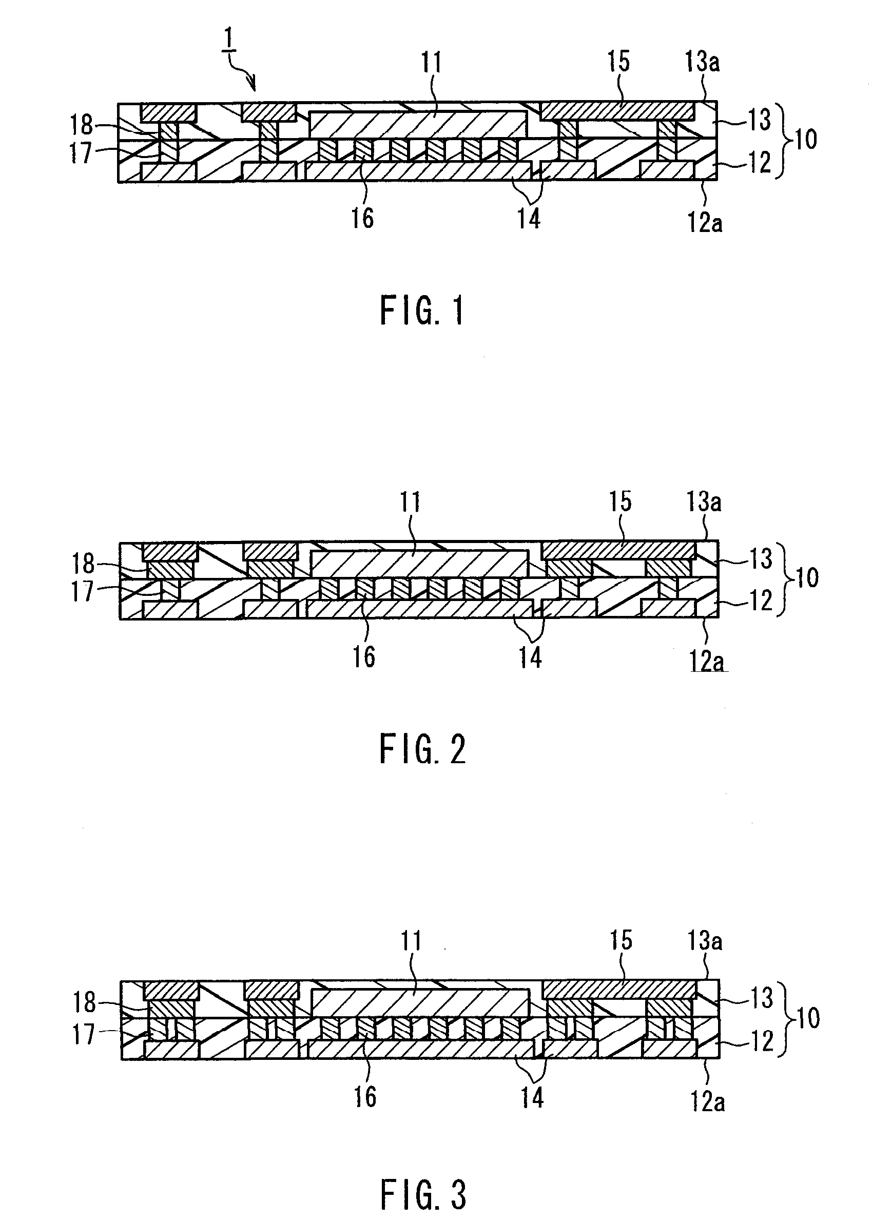
[0064]First, an electronic component embedded module according to a First Embodiment of the present invention will be described. FIG. 1 is a cross-sectional view showing an electronic component embedded module according to First Embodiment of the present invention.

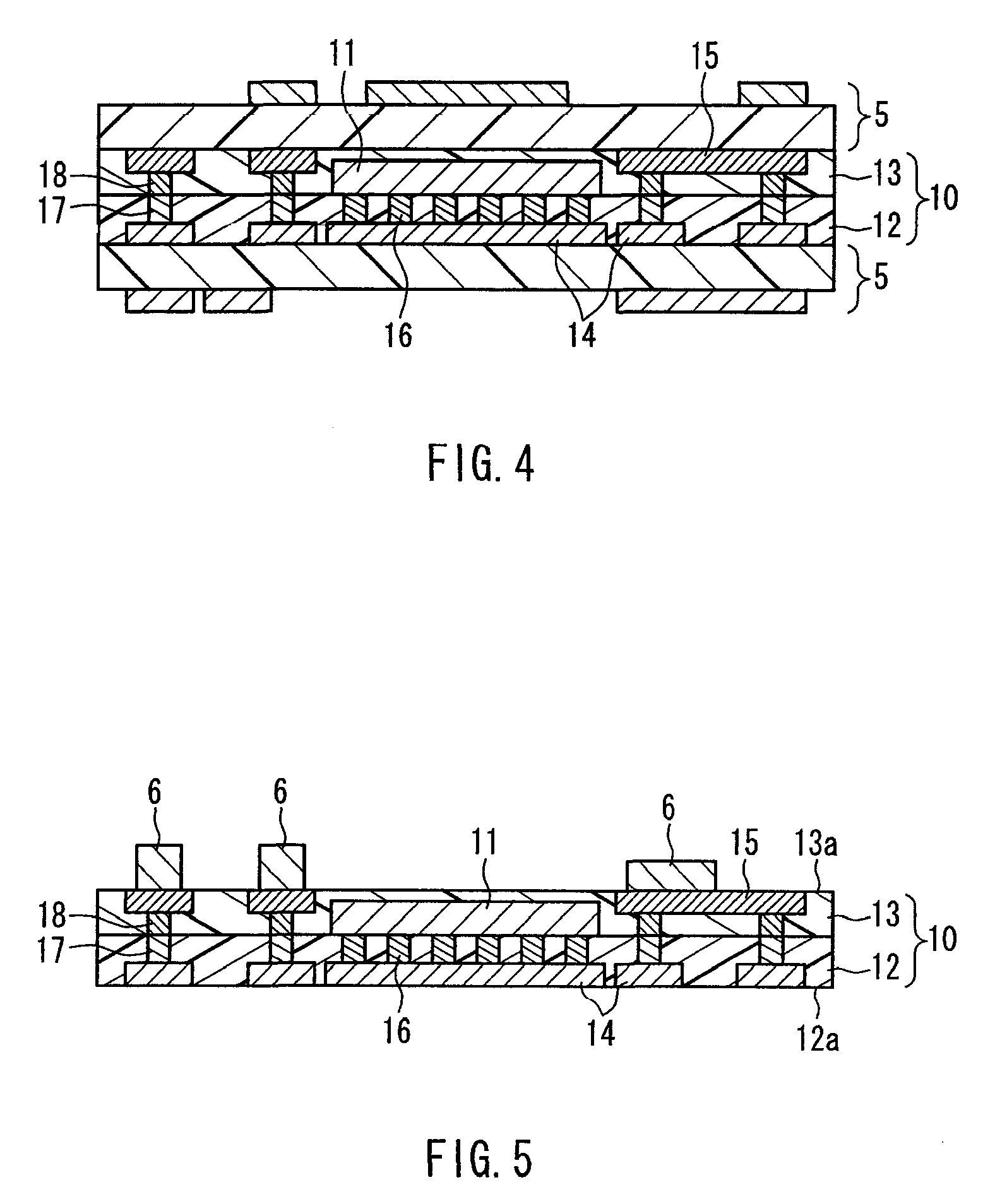
[0065]As shown in FIG. 1, an electronic component embedded module 1 includes an electrical insulating substrate 10 and a first electronic component 11 embedded in the electrical insulating substrate 10. The electrical insulating substrate 10 includes a first electrical insulating layer 12 and a second electrical insulating layer 13 laminated on the first electrical insulating layer 12. A first wiring pattern 14 is disposed on a main face 12a of the first electrical insulating layer 12 opposite to the second electrical insulating layer 13. A second wiring pattern 15 is disposed on a main face 13a of the second electrical insulating layer 13 opposite to the first electrical insulating layer 12. It is preferable that the thic...

second embodiment

[0084]The following description is about an electronic component embedded module according to Second Embodiment of the present invention. FIG. 7 is a cross-sectional view showing the electronic component embedded module according to Second Embodiment.

[0085]As shown in FIG. 7, an electronic component embedded module 2 includes an electrical insulating substrate 100, and a first electronic component 101a and a second electronic component 101b embedded in the electrical insulating substrate 100. The electrical insulating substrate 100 includes a first electrical insulating layer 102, a second electrical insulating layer 103, and a third electrical insulating layer 150 sandwiched by the first and second electrical insulating layers 102, 103. A first wiring pattern 104 is disposed on a main face 102a of the first electrical insulating layer 102 opposite to the third electrical insulating layer 150. A second wiring pattern 105 is disposed on a main face 103a of the second electrical insul...


PUM


Abstract

An electronic component embedded module that can improve reliability of electric connection of inner vias, and a manufacturing method therefor are provided. A first electronic component (11) is embedded in a second electrical insulating layer (13) and connected electrically to a first wiring pattern (14) through first inner vias (16) that penetrate a first electrical insulating layer (12). The first wiring pattern (14) and a second wiring pattern (15) are connected electrically to each other through second inner vias (17) that penetrate the first electrical insulating layer (12) and third inner vias (18) that penetrate the second electrical insulating layer (13). The second inner vias (17) and the third inner vias (18) are arranged continuously.

Description

TECHNICAL FIELD[0001]The present invention relates to an electronic component embedded module that embeds an electronic component, and a method for manufacturing the same.BACKGROUND ART[0002]With the recent trend for smaller and lightweight electronic equipment, demands for high-density printed circuit boards and small surface-mounted components have become stricter. For the printed circuit boards, efforts have been made to increase the density in a direction parallel to the circuit board surface by narrowing the wiring rule. Further, a buildup method is employed to laminate circuit boards, and inner vias are formed perpendicular to the circuit board surfaces.[0003]For the purpose of providing smaller surface-mounted components, a CSP (Chip Size Package) has been used widely. This is prepared by flip-chip mounting an active element side of a semiconductor chip to face a circuit board. In the flip chip mounting, a semiconductor bare chip is mounted directly on a circuit board through...

Claims


Application Information

Patent Timeline
Patent Type & Authority Applications(United States)
IPC IPC(8): H01L23/52H01L21/44
CPCH01L23/5389H01L25/0657H01L2224/82047H01L2225/06524H01L2224/16235H01L2225/06582H01L2924/01078H01L2924/01079H01L2225/06541
Inventor OKIMOTO, RIKIYAKOJIMA, TOSHIYUKIISHIMARU, YUKIHIRO
Owner PANASONIC CORP
Learn More