Eureka AIR delivers breakthrough ideas for toughest innovation challenges, trusted by R&D personnel around the world.

Ultrathin semiconductor chip packaging structure and manufacturing process thereof

A technology of chip packaging structure and manufacturing process, which is applied in semiconductor/solid-state device manufacturing, semiconductor devices, semiconductor/solid-state device components, etc., can solve the problem of reducing the width of chip cutting lines, limiting the number of packaged chip pads, and increasing packaging Solve the overall thickness and volume of the structure to achieve the effect of reducing the packaging volume and improving the reliability of electrical connection

Active Publication Date: 2010-07-28
CHINA WAFER LEVEL CSP
View PDF3 Cites 10 Cited by
  • Summary
  • Abstract
  • Description
  • Claims
  • Application Information

AI Technical Summary

Problems solved by technology

[0003] The chip packaging structure manufactured by conventional wafer-level chip size packaging technology usually only uses a single layer of leads. Due to the limited space on the soldering bump surface, the number of solder pads of the packaged chip is limited.
The current idea is to use a double-layer lead package structure in order to save more space on the solder bump surface of the packaged chip for lead layout, thereby allowing more pads per unit area (for example, the pads are arranged in a double row) However, the existing technical problem is that the use of double-layer leads will inevitably further increase the overall thickness and volume of the package structure; and the excessively thick package thickness is not conducive to the reduction of the width of the dicing lines between chips, thus It is impossible to manufacture more chips on the same size wafer, resulting in greatly reduced wafer utilization and increased packaging costs
In short, the existing wafer-level chip size packaging technology is still unable to implement effective packaging for multi-pad chips (such as chips with dual-row array of pads), which has great limitations.

Method used


Image

  • Ultrathin semiconductor chip packaging structure and manufacturing process thereof
  • Ultrathin semiconductor chip packaging structure and manufacturing process thereof
  • Ultrathin semiconductor chip packaging structure and manufacturing process thereof

Examples


Embodiment

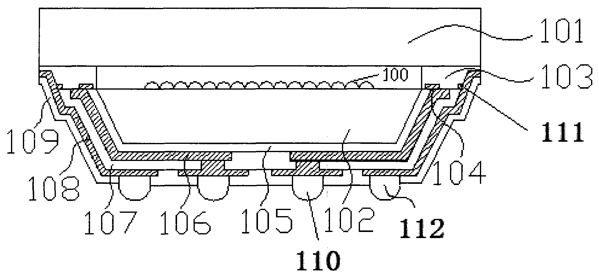
[0035] Example: such as figure 1 As shown, in the ultra-thin semiconductor chip packaging structure provided in this embodiment, the front side of the chip 102 is provided with soldering pads and photosensitive devices 100, and the soldering pads are arranged in double rows around the chip 102, and the inner ones are The first row of welding pads 104, and the second row of welding pads 111 located on the outside, and the two rows of welding pads are electrically connected with the chip 102 through the circuit (not shown in the figure); and the glass substrate 101 described in the present embodiment A cavity wall 103 in a closed-loop structure is provided on it, and the front surface of the chip 102 is pressed against the cavity wall 103 on the glass substrate 101 to form a cavity surrounding the photosensitive device 100 . A first insulating layer 105 is directly deposited on the back of the chip 102, a first wiring layer 106 is deposited on the back of the first insulating la...


PUM


Abstract

The invention discloses an ultrathin semiconductor chip packaging structure, wherein double-layer leads are adopted for packaging a chip with a weld pad in double-row arrangement, and the two paths of leads do not mutually interfere, thereby further improving the reliability of electric connection; meanwhile, compared with the prior art, a single-side polymer is adopted for replacing the glass on the back surface of an original chip, a glass-silicon-polymer structure is adopted, the packaging thickness is further thinned, and the thickness can be reduced from the original 0.9mm to 0.5mm when in practical application, thereby greatly reducing the packaging volume of a semiconductor chip.

Description

technical field [0001] The invention relates to an ultra-thin semiconductor chip packaging structure and a manufacturing process thereof. Background technique [0002] The current wafer-level chip size packaging technology is to package and test the entire wafer, and then cut it to obtain a single chip. It adopts a glass-silicon-glass sandwich structure, and the packaged product size reaches 1: 1.3, is recognized by the industry as the world's leading semiconductor packaging technology. [0003] The chip packaging structure manufactured by the conventional wafer-level chip size packaging technology usually only uses a single-layer lead, and the number of pads of the packaged chip is limited due to the limited space on the soldering bump. The current idea is to use a double-layer lead package structure in order to save more space on the solder bump surface of the packaged chip for lead layout, thereby allowing more pads per unit area (for example, the pads are arranged in a ...

Claims


Application Information

Patent Timeline
Patent Type & Authority Applications(China)
IPC IPC(8): H01L23/485H01L23/29H01L21/50H01L21/56H01L21/60
CPCH01L2224/10
Inventor 王卓伟俞国庆邹秋红王蔚
Owner CHINA WAFER LEVEL CSP
Why Eureka
Eureka Blog
Learn More