Laminated inductor and method of manufacture of same

a technology of inductor and laminate, which is applied in the direction of inductance, magnets, magnetic bodies, etc., can solve the problems of small cracking, small cracking, and small cracking in the portion of the laminate positioned, so as to reduce the concern of short-circuit between adjacent conductor patterns due to the migration phenomenon, and the tendency to reduce the tendency to break

Active Publication Date: 2009-05-07
TDK CORPARATION
View PDF4 Cites 19 Cited by
  • Summary
  • Abstract
  • Description
  • Claims
  • Application Information

AI Technical Summary

Benefits of technology

[0021]In a method of manufacturing a laminated inductor of this invention, the mth ceramic film is formed so as to cover the edge portions of the mth conductive film and expose the upper face of the mth conductive film other than the edge portions, the nth conductive film is formed on the exposed face of the mth conductive film and the mth ceramic film with the same pattern as the mth conductive film, and the nth ceramic film is formed so as to cover the edge portions of the nth conductive film and expose the upper face of the nth conductive film other than the edge portions. Hence, by means of a method of manufacture of laminated inductors of this invention, the peripheral side faces of the conductor pattern are formed as concavo-convex faces in which concave portions and convex portions are alternated in the lamination direction, and a laminated inductor can be manufactured with the laminate entering into the concave portions of the peripheral side faces. As a result, due to the so-called anchor effect, there is extremely little tendency for separation of the laminate from the depression/protrusion shape peripheral side faces, and so there is very little tendency for cracking to occur in the portions of the laminate positioned between adjacent conductor patterns in the lamination direction. Hence, concerns about short-circuits between adjacent conductor patterns due to the migration phenomenon are greatly reduced.
[0022]Further, in a method of manufacture of laminated inductors of this invention, the nth ceramic film is formed such that the edge portions of the nth conductive film are covered and the upper face of the conductive film other than the edge portions is exposed, and such that the height of the nth ceramic film from the green sheet is greater than the height of the nth conductive film from the green sheet. Hence, compared with manufacturing methods of the prior art in which an auxiliary magnetic material layer was formed so as to surround the perimeter of the conductor pattern, when a plurality of green sheets are laminated, the area of contact between the nth ceramic film formed on one green sheet and other

Problems solved by technology

However, when adopting a method of electronic component manufacture of the prior art, in general the conductive paste and the green sheet are prepared such that the shrinkage rate of the conductive paste during burning is greater than the shrinkage rate of the green sheet during burning; and so to the extent that the conductor pattern thickness is increased, a gap tends to occur between the peripheral side faces of the conductor pattern in the manufactured laminated inductor and the portions of the laminate in contact with the side faces.
For this

Method used


Image

  • Laminated inductor and method of manufacture of same
  • Laminated inductor and method of manufacture of same
  • Laminated inductor and method of manufacture of same

Examples


Embodiment Construction

[0036]Preferred embodiments of the invention are explained referring to the drawings. In the explanations, the same symbols are used for the same elements or for elements having the same functions, and redundant explanations are omitted.

[0037]Configuration of Laminated Inductor

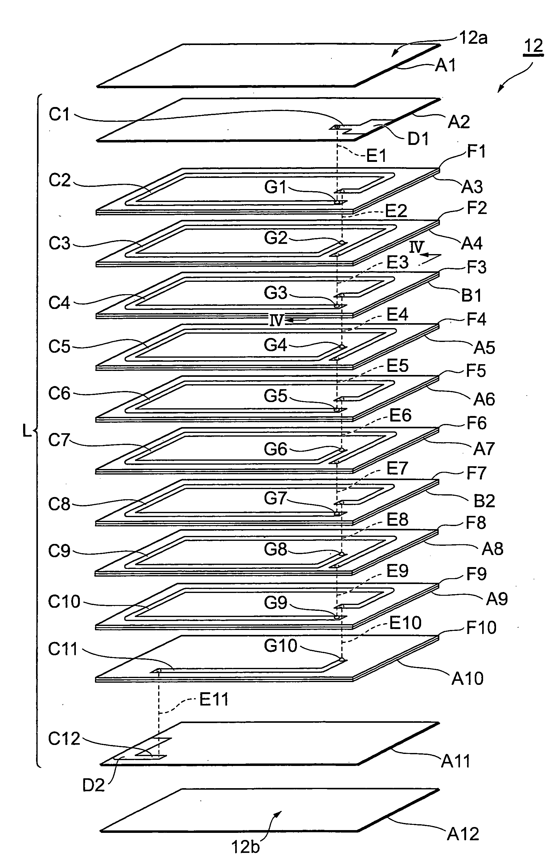
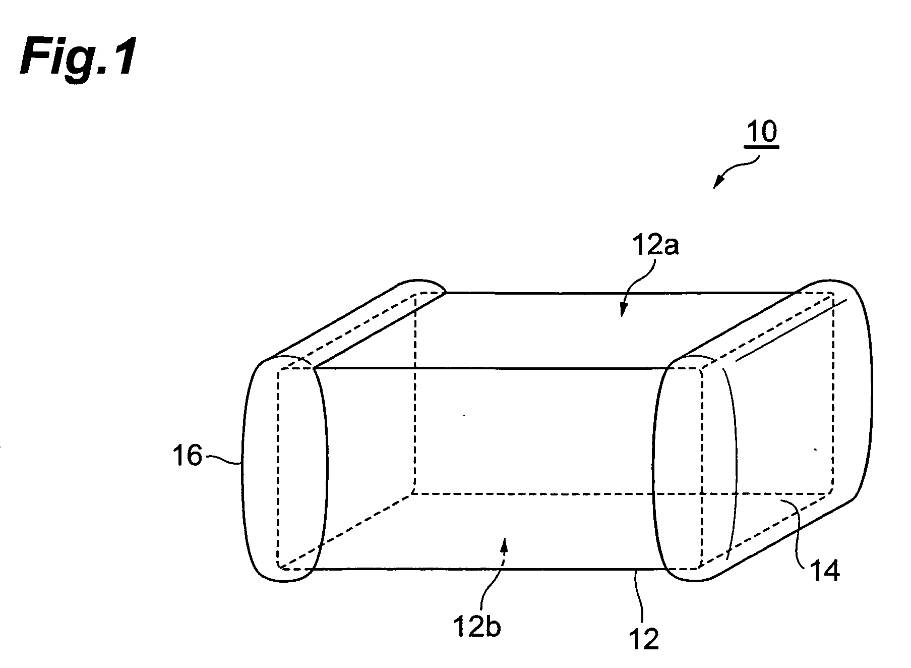
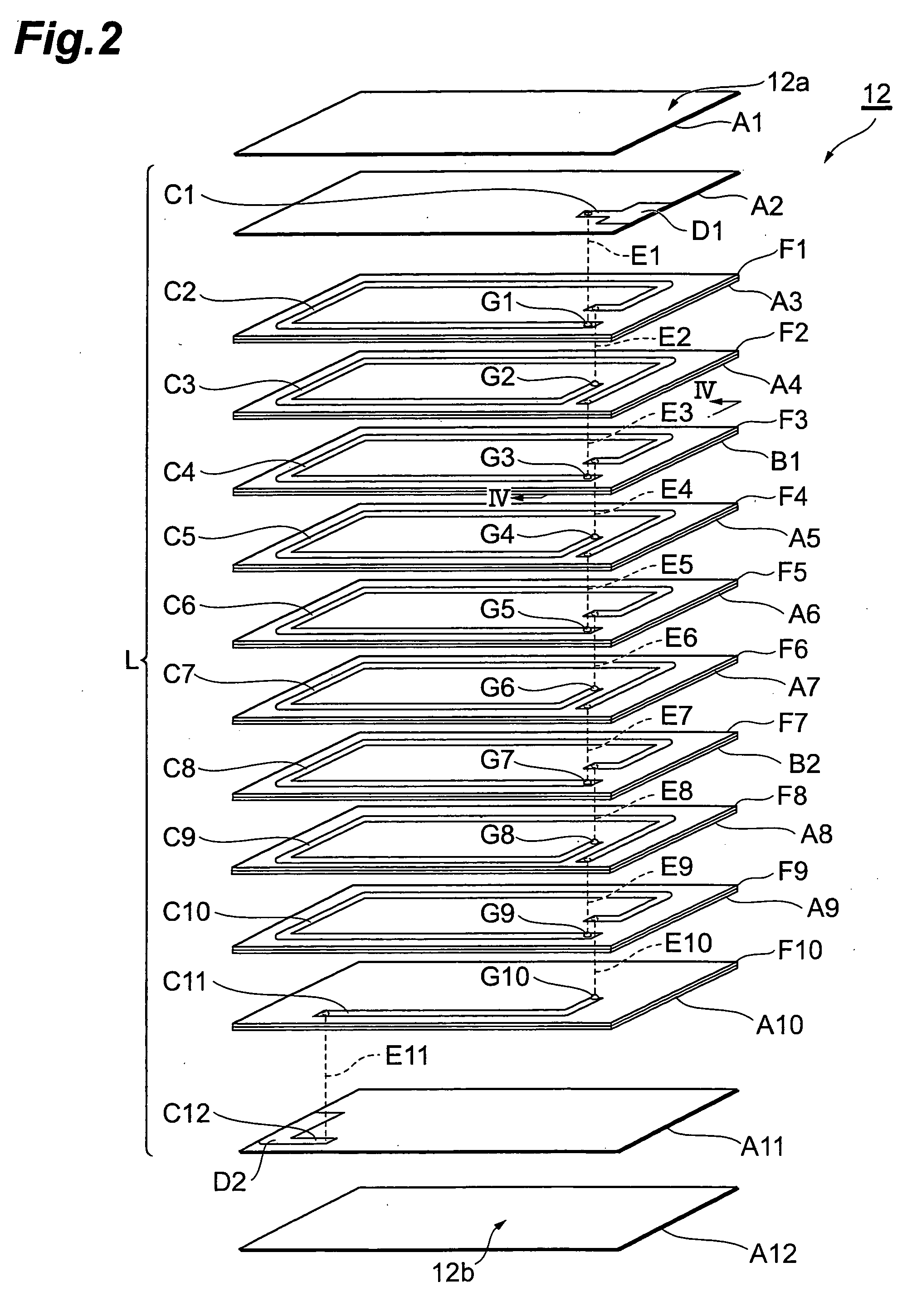
[0038]First, the configuration of the laminated inductor 10 of an embodiment is explained, referring to FIG. 1 to FIG. 5. As shown in FIG. 1 and FIG. 2, the laminated inductor 10 comprises a laminate 12 with substantially a rectangular parallelepiped shape; a pair of external electrodes 14 and 16, formed on the two peripheral side faces respectively in the length direction of the laminate 12; and a coil L, formed by electrically connecting each of conductor patterns C1 to C12 within the laminate 12.

[0039]The laminate 12 has a pair of main faces 12a, 12b, which are opposed so as to be substantially parallel. One among the main faces 12a, 12b is a face which, when the laminated inductor 10 is mounted on an exter...


PUM

PropertyMeasurementUnit
Lengthaaaaaaaaaa
Widthaaaaaaaaaa
Widthaaaaaaaaaa

Abstract

A laminated inductor, in which there is extremely little tendency for cracking to occur between adjacent conductor patterns in portions of a laminate in the lamination direction even when the conductor pattern thickness is large, as well as a method of manufacturing such a laminated inductor, are provided.
A laminated inductor includes: a laminate; a pair of external electrodes arranged on the outer surfaces of the laminate respectively; and a coil, arranged within the laminate and formed by electrically connecting a plurality of strip-like conductor patterns. The conductor patterns have: a pair of broad faces, intersecting the lamination direction and mutually opposing; and peripheral side faces adjacent to the pair of broad faces and extending in the lamination direction. The peripheral side faces are concavo-convex faces, in which concave portions and convex portions are arranged in alternation in the lamination direction. The laminate enters into the concave portions of the peripheral side faces.

Description

BACKGROUND OF THE INVENTION[0001]1. Field of the Invention[0002]This invention relates to a laminated inductor, and to a method of manufacture of a laminated inductor.[0003]2. Related Background Art[0004]In the prior art, methods are known for the manufacture of couplers and other electronic components in which laser light is used to form grooves in a green sheet, and the grooves are filled with a conductive paste, for the purpose of increasing the thickness of the conduction pattern and reducing electrical resistance (see for example Patent Literature 1). An electronic component manufactured by such a method of electronic component manufacture comprises a laminate, in which a plurality of insulator layers are laminated, and a strip-like conductor pattern positioned within the laminate. The conductor pattern has a pair of broad faces, and peripheral side faces which connect the pair of broad faces over the entire perimeter of the pair of broad faces.[0005]Patent Literature 1: Japane...

Claims


Application Information

Patent Timeline
IPC IPC(8): H01F5/00
CPCH01F17/0013Y10T29/4902H01F2017/0066H01F27/2804H01F2027/2809
Inventor ARATA, MASAZUMIKAWASAKI, KUNIHIKOODA, KUNIOTADAKI, YOHEISATOH, YOSHIMITSUSASAKI, HITOSHI
Owner TDK CORPARATION
Why Eureka
Try Eureka