Eureka AIR delivers breakthrough ideas for toughest innovation challenges, trusted by R&D personnel around the world.

Method of correcting mask pattern, photo mask, method of manufacturing semiconductor device, and semiconductor device

Inactive Publication Date: 2009-05-07
SHARP KK
View PDF3 Cites 4 Cited by
  • Summary
  • Abstract
  • Description
  • Claims
  • Application Information

AI Technical Summary

Benefits of technology

[0018]With this arrangement, before carrying out the micro-fabrication process, the mask pattern of the mask used in the micro-fabrication process is corrected so that the etching proximity effect is dealt with, by use of the correction model in which the pattern size and the inter-pattern space size are set as the parameters. In addition, since the pattern size and the inter-pattern space size are set as the parameters in the correction model, the correction model is prepared accurately. Thus, the mask pattern can be corrected with high accuracy so that a wiring pattern having desired dimensions is formed on the substrate, thereby dealing with the etching proximity effect.
[0020]With this arrangement, since the pattern size and the inter-pattern space size are set as the parameters in the correction model, the correction model is prepared accurately. Thus, it is possible to realize the mask having the mask pattern that is corrected with high accuracy so that a wiring pattern having desired dimensions is formed on the substrate, thereby dealing with the etching proximity effect.
[0022]With this arrangement, the mask is formed, the mask having the mask pattern that has been subjected to the correction so that the etching proximity effect is dealt with, by use of the correction model in which the pattern size and the inter-pattern space size are set as the parameters. Then, the wiring pattern is formed on the substrate in the micro-fabrication process, by use of the mask. In addition, since the pattern size and the inter-pattern space size are set as the parameters in the correction model, the correction model is prepared accurately. Thus, it is possible to form the wiring pattern having desired dimensions on the substrate with high accuracy.
[0024]With this arrangement, since the pattern size and the inter-pattern space size are set as the parameters in the correction model, the correction model is prepared accurately. By this, the mask pattern of the mask is corrected with high accuracy so that the etching proximity effect is dealt with. Thus, it is possible to realize a semiconductor device, on the substrate of which the wiring pattern having the desired dimensions is formed with high accuracy.

Problems solved by technology

Therefore, according to the art disclosed in the publicly known document 1, it is not possible to prepare a highly accurate etching proximity effect correction model.
This causes a problem that it is not possible to form, with accurate dimensions as designed, an ultimate wiring pattern on the substrate of a semiconductor device.

Method used


Image

  • Method of correcting mask pattern, photo mask, method of manufacturing semiconductor device, and semiconductor device
  • Method of correcting mask pattern, photo mask, method of manufacturing semiconductor device, and semiconductor device
  • Method of correcting mask pattern, photo mask, method of manufacturing semiconductor device, and semiconductor device

Examples


Embodiment Construction

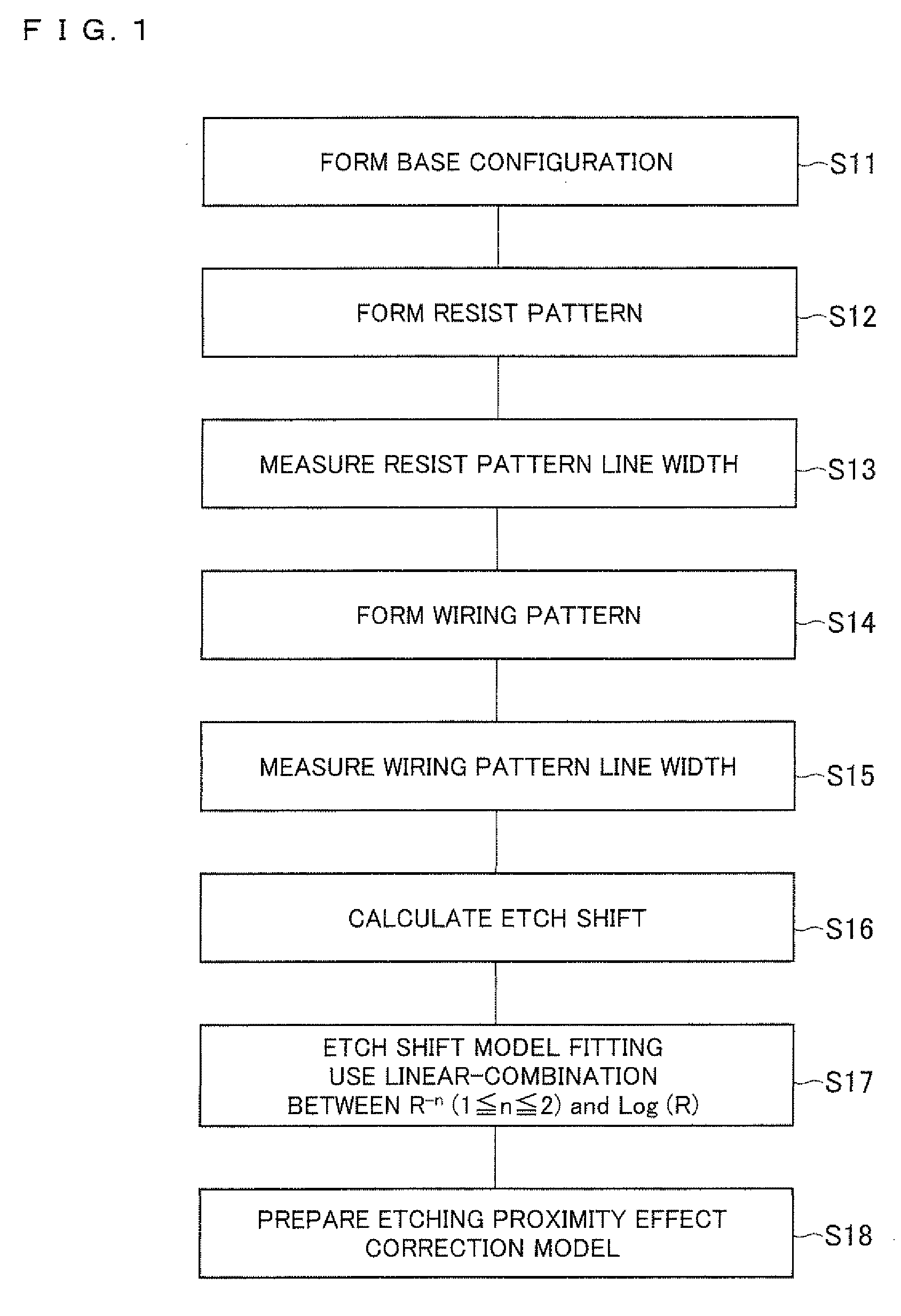
[0040]One embodiment of the present invention is described below with reference to drawings.

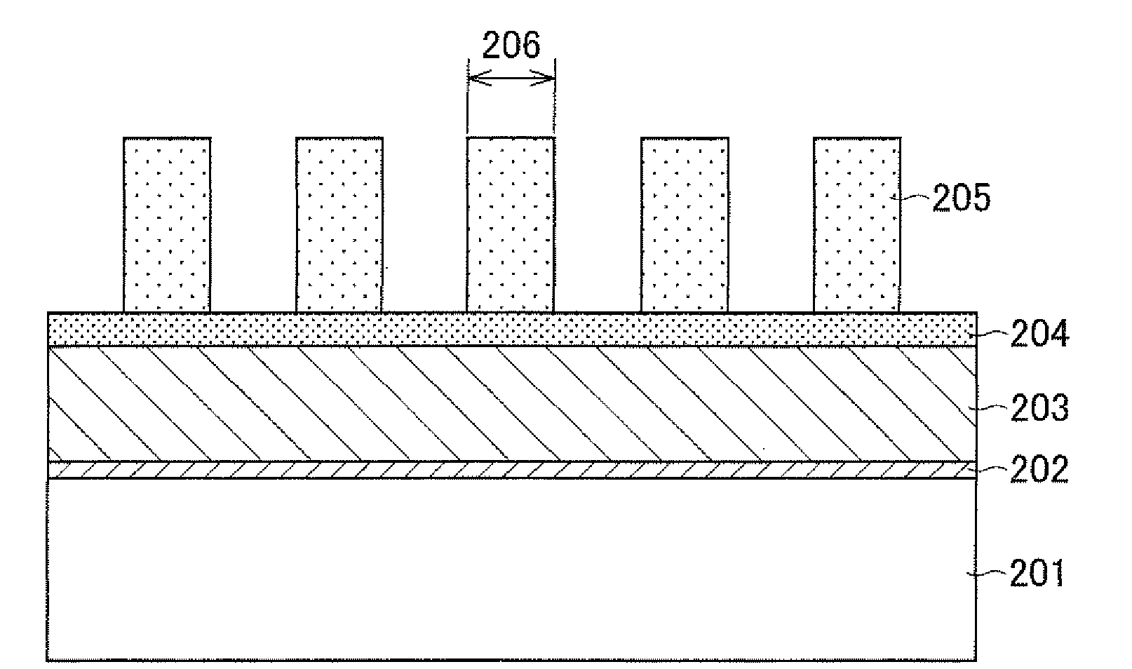
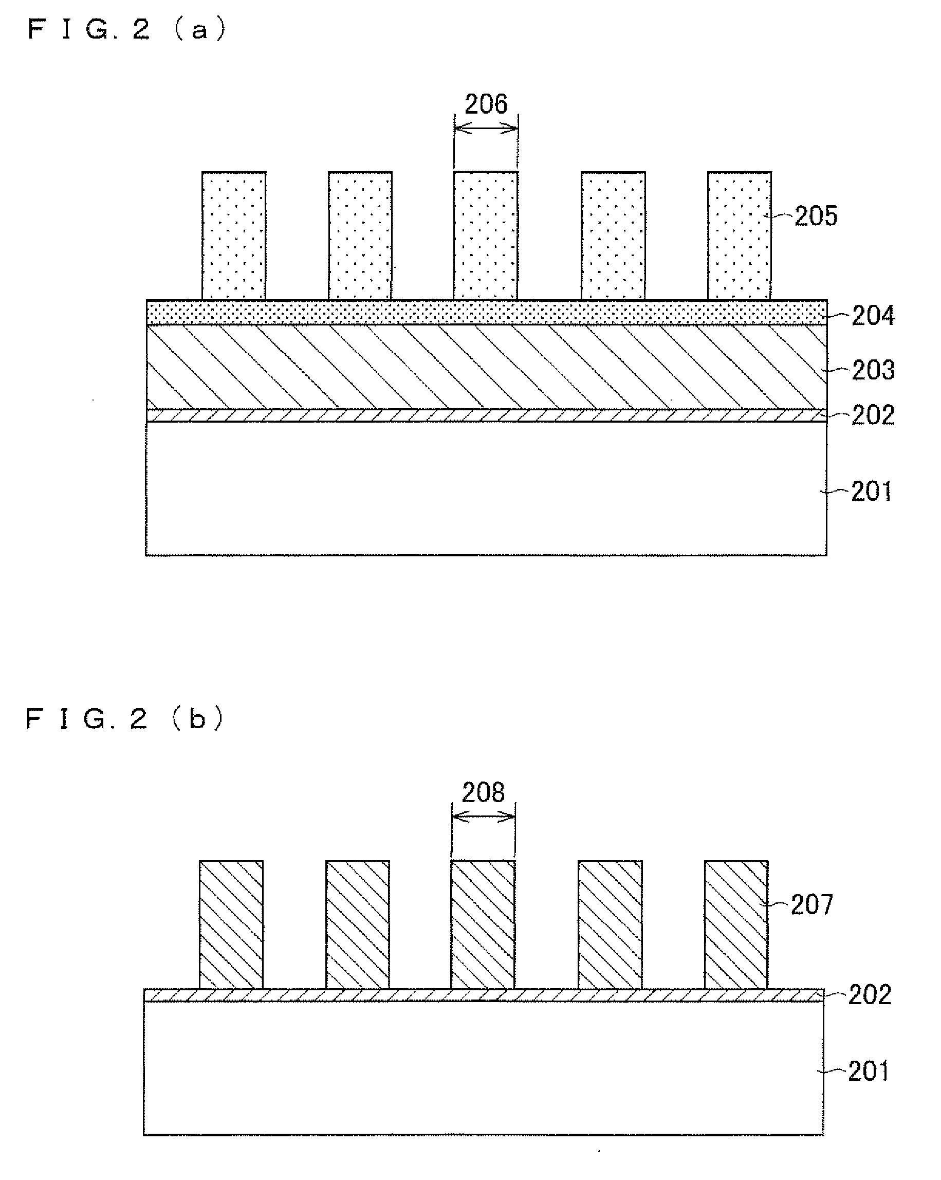
[0041]A method for correcting a mask pattern in accordance with the present invention is a method capable of correcting a mask pattern to deal with the etching proximity effect, by use of a highly accurate etching proximity effect correction model, so that the wiring pattern having desired dimensions is ultimately formed on a substrate. The following description first deals with a preparing process (method) of an etching proximity effect correction model used in a method for correcting a mask pattern in accordance with the present embodiment, and then deals with a method of manufacturing a semiconductor device, in which method a mask corrected by the method of correcting the mask pattern is used. The following description deals with a case, as an example, in which a method for correcting the mask pattern in accordance with the present embodiment is applied to a mask pattern of a gate.

[0042][A...


PUM

PropertyMeasurementUnit
Sizeaaaaaaaaaa
Dimensionaaaaaaaaaa

Abstract

A method of correcting a mask pattern, the method correcting the mask pattern of a mask such that a wiring pattern having desired dimensions is formed based on a micro-fabrication process using the mask, corrects the mask pattern so that, before carrying out the micro-fabrication process, an etching proximity effect is dealt with by use of the correction model in which a pattern size and a inter-patter space size are set as parameters. This makes it possible to correct the mask pattern with high accuracy so that the wiring pattern having the desired dimensions is formed on the substrate, thereby dealing with the etching proximity effect.

Description

[0001]This Nonprovisional application claims priority under 35 U.S.C. § 119(a) on Patent Application No. 290134 / 2007 filed in Japan on Nov. 7, 2007, the entire contents of which are hereby incorporated by reference.FIELD OF THE INVENTION[0002]The present invention relates to a method of correcting a mask pattern in manufacture of a semiconductor device, a photo mask manufactured by this method, a method of manufacturing a semiconductor device, a semiconductor device manufactured by this method, and more particularly to art directed to an improvement in deterioration of accuracy of a fine pattern formation caused by a process proximity effect.BACKGROUND OF THE INVENTION[0003]As an improvement in speed and high integration of semiconductor devices have been advanced today, fine transistors and fine wiring patterns have been required. In this regard, downsizing of gate dimensions is particularly known to be effective in an improvement in speed and high integration of the transistors. A...

Claims


Application Information

Patent Timeline
IPC IPC(8): B32B5/00G03F1/00G03F7/20G03F1/36G03F1/68G03F1/80H01L21/027
CPCG03F1/144Y10T428/24802G03F1/36G03F1/80
Inventor TAMURA, KOJI
Owner SHARP KK
Why Eureka
Eureka Blog
Learn More