Manufacturing method of semiconductor integrated device

a manufacturing method and integrated device technology, applied in coatings, electrolysis components, electrolysis processes, etc., can solve the problems of precipitate attachment to the wafer, affecting the production efficiency of the product, so as to achieve efficient dissolving/discharging of precipitate in the plating. , the effect of preventing the abnormal growth of projections on the gold bump electrod

Inactive Publication Date: 2009-05-07
RENESAS ELECTRONICS CORP
View PDF4 Cites 19 Cited by
  • Summary
  • Abstract
  • Description
  • Claims
  • Application Information

AI Technical Summary

Benefits of technology

[0016]Abnormal growth of projections on a gold bump electrode is prevented by carrying out for each wafer to be treated, prior to a gold bump / plating step, a step of circulating and stirring a plating solution while erecting a plating cup and efficiently dissolving / discharging a precipitate in the plating solution.

Problems solved by technology

The projections on the bump electrode become a significant barrier to mounting work.
When a subsequent plating operation is started before the precipitate does not dissolve sufficiently in the plating solution, the precipitate attaches to the wafer and becomes a nucleus of abnormally growing projection.
It has been found that only extension of an ordinary stirring time performed prior to plating is almost useless for dissolving the precipitate.

Method used


Image

  • Manufacturing method of semiconductor integrated device
  • Manufacturing method of semiconductor integrated device
  • Manufacturing method of semiconductor integrated device

Examples


embodiment

Outline of Embodiment

[0057]First, the outline of typical embodiments of the invention disclosed herein will be described.

[0058]1. A manufacturing method of a semiconductor integrated circuit device comprises the steps of:

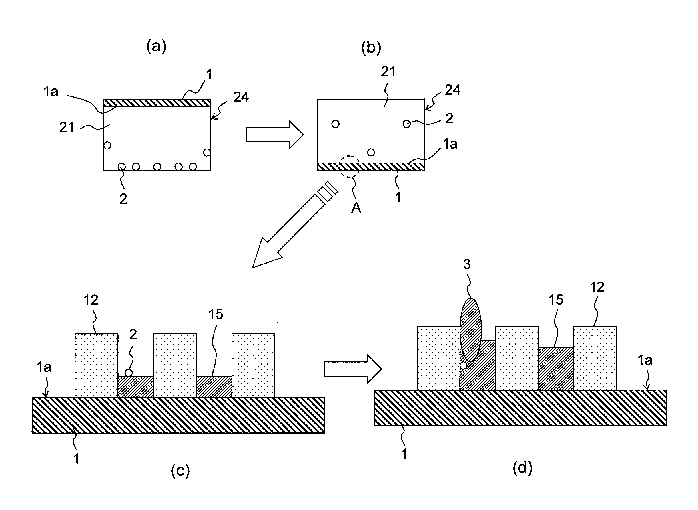
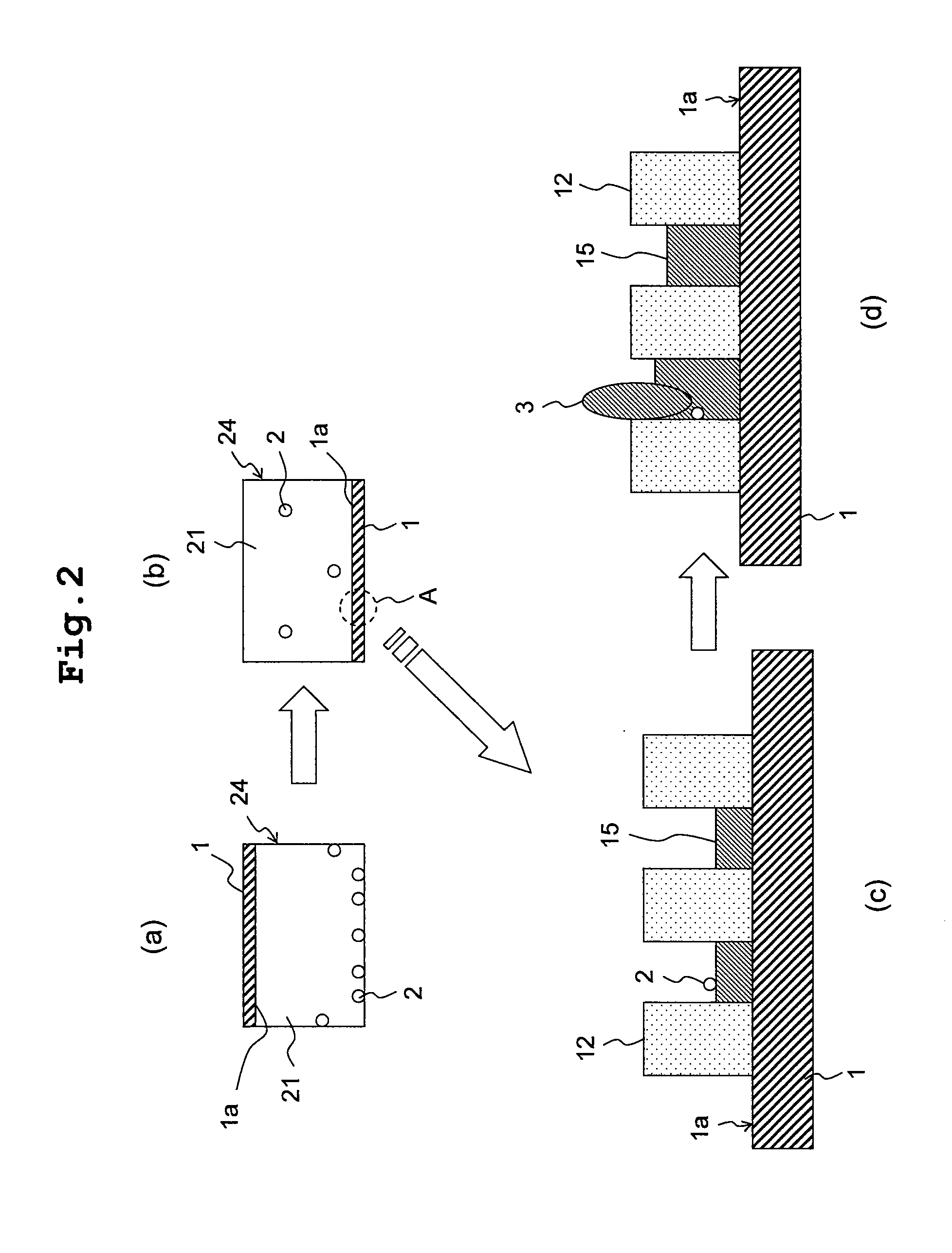
[0059](a) forming a resist film having a plurality of openings over a first main surface of a wafer;

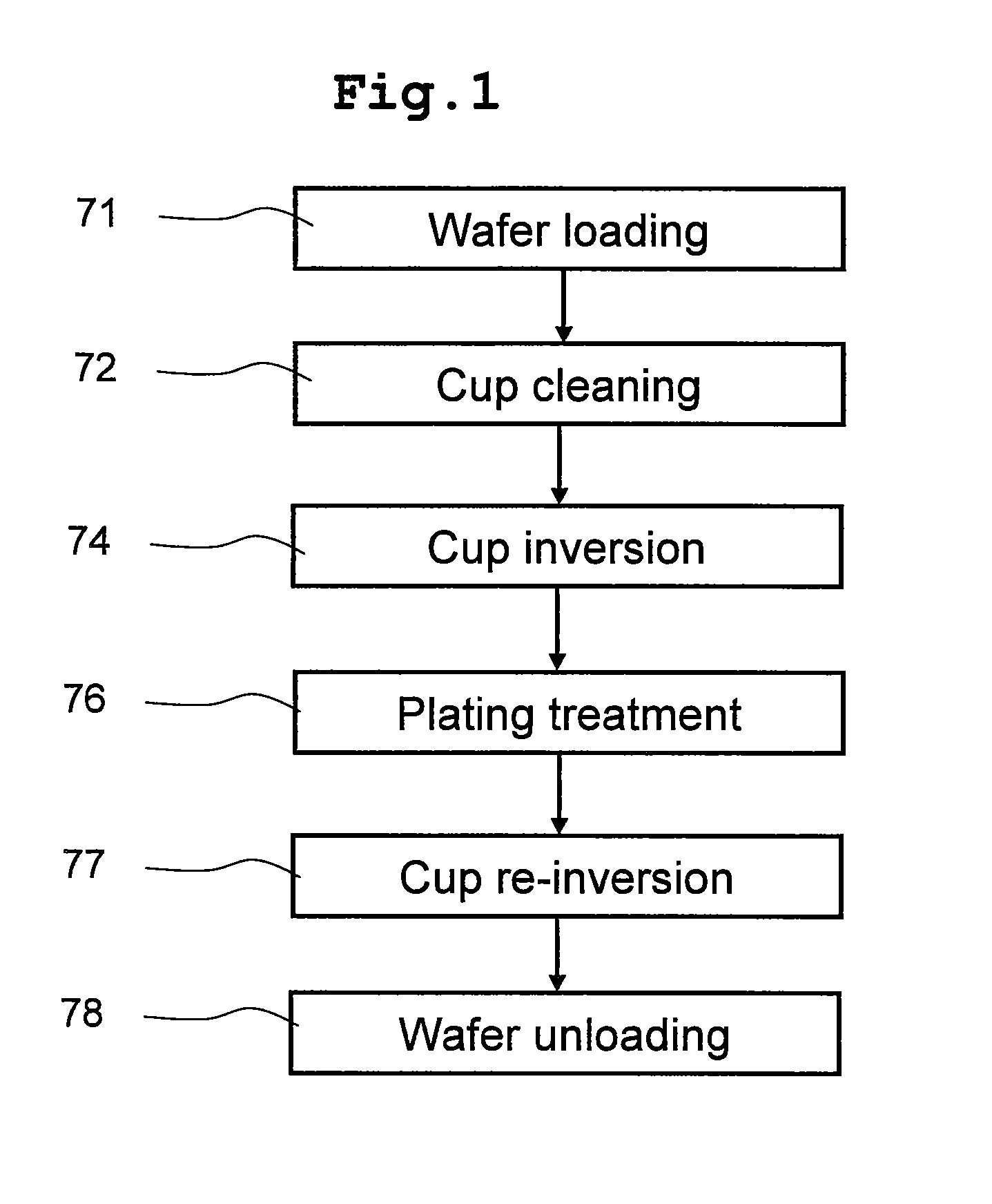
[0060](b) introducing the wafer having the resist film into a single-wafer plating apparatus having a plating cup;

[0061](c) loading, in the single-wafer plating apparatus, the wafer having the resist film in the plating cup so that the first main surface lies opposite to a plating tank of the plating cup;

[0062](d) after the step (b), introducing a plating solution into the plating tank;

[0063](e) after the step (d), stirring the plating solution in the plating tank;

[0064](f) after the steps (c) and (e), forming a gold bump electrode by electroplating over the opening portions over the first main surface; and

[0065](g) after the step (f), unloading the wafer from the pla...


PUM

PropertyMeasurementUnit
sizeaaaaaaaaaa
thicknessaaaaaaaaaa
thicknessaaaaaaaaaa

Abstract

Manufacture of semiconductor products such as LCD driver requires a bump plating step for forming a gold bump electrode having a size of from about 15 to 20 μm. This bump plating step is performed by electroplating with a predetermined plating solution, but projections intermittently appear on the bump electrode during a mass production process. In the invention, abnormal growth of projections over the gold bump electrode is prevented by adding, prior to the gold bump plating step, a step of circulating and stirring a plating solution while erecting a plating cup and efficiently dissolving/discharging a precipitate. This step is performed for each wafer to be treated.

Description

CLAIM OF PRIORITY[0001]The Present application claims priority from Japanese application JP 2007-285969 filed on Nov. 2, 2007, the content of which is hereby incorporated by reference into this application.FIELD OF THE INVENTION[0002]The present invention relates to a bump formation technology in manufacturing methods of a semiconductor integrated circuit device (or a semiconductor device). In particular, the invention pertains to a technology effective when applied to a gold bump formation technology.BACKGROUND OF THE INVENTION[0003]Japanese Unexamined Patent Publication No. Hei 8(1996)-311699 (Patent Document 1) discloses a technology of stirring a plating solution present in the vicinity of a wafer with a view to minimizing unevenness of a plating thickness during electroplating of the wafer.[0004]Japanese Unexamined Patent Publication No. 2006-22379 (Patent Document 2) discloses, in gold electroplating for the formation of a bump electrode of a wafer or the like, an electroplati...

Claims


Application Information

Patent Timeline
Patent Type & Authority Applications(United States)
IPC IPC(8): H01L21/44
CPCH01L24/03H01L24/11H01L2924/0002H01L2224/03912H01L2224/0401H01L2224/05572H01L2224/1147H01L2224/11912H01L2224/13099H01L2224/13144H01L2224/16H01L2924/01004H01L2924/01005H01L2924/01007H01L2924/01011H01L2924/01013H01L2924/01014H01L2924/01015H01L2924/01022H01L2924/01027H01L2924/01029H01L2924/01033H01L2924/01046H01L2924/01047H01L2924/01049H01L2924/0105H01L2924/01057H01L2924/01075H01L2924/01077H01L2924/01078H01L2924/01079H01L2924/014H01L2924/05042H01L2924/14H01L2924/30105H01L2924/01006H01L2924/01019H01L2224/02166H01L2224/05553H01L2224/05552
Inventor MAITANI, TOTAKANAOKA, TAKU
Owner RENESAS ELECTRONICS CORP
Why Eureka
Try Eureka